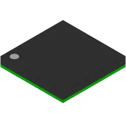
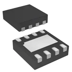
規格
| Brand | AMD / Xilinx |
| Product Type | FPGA - Configuration Memory |
| Subcategory | Programmable Logic ICs |
| Factory Pack Quantity:Factory Pack Quantity | 74 |
概述
Description
XCF04S is a field-programmable gate array (FPGA) from Xilinx’s Spartan series, designed for cost-effective, low-power applications. It features a 4-input LUT architecture, enabling flexibility in digital design. The device supports various I/O standards, allowing seamless integration with different systems. With up to 1,024 logic cells and multiple DSP slices, it provides sufficient resources for a range of applications, including embedded processing and communication systems.
XCF04S is particularly beneficial for prototyping and low-volume production due to its reconfigurability, which allows designers to modify the hardware as needed without changing the physical device. Its compatibility with Xilinx’s Vivado Design Suite ensures efficient design and synthesis processes.
Overall, the XCF04S is an ideal choice for developers seeking a balance between performance, power consumption, and cost in their digital circuit designs.
XCF04S is particularly beneficial for prototyping and low-volume production due to its reconfigurability, which allows designers to modify the hardware as needed without changing the physical device. Its compatibility with Xilinx’s Vivado Design Suite ensures efficient design and synthesis processes.
Overall, the XCF04S is an ideal choice for developers seeking a balance between performance, power consumption, and cost in their digital circuit designs.
Features
The XCF04S is a versatile FPGA (Field Programmable Gate Array) from Xilinx, designed for various applications in embedded systems and digital signal processing. Key features include:
1. Capacity: It offers a logic cell count suitable for moderate complexity designs.
2. I/O Configuration: Supports multiple I/O standards, allowing flexibility in interfacing with other components.
3. Embedded Memory: Includes block RAM for efficient data storage and retrieval.
4. DSP Slices: Contains dedicated DSP slices for high-performance arithmetic operations, ideal for signal processing tasks.
5. Power Efficiency: Designed for low power consumption, making it suitable for battery-operated devices.
6. Development Tools: Compatible with Xilinx’s Vivado Design Suite, facilitating easier design and implementation.
7. Configurable Logic: Users can customize the logic architecture to meet specific application needs.
Overall, the XCF04S is suitable for applications in telecommunications, automotive, and consumer electronics, providing a balance of performance, flexibility, and efficiency.
1. Capacity: It offers a logic cell count suitable for moderate complexity designs.
2. I/O Configuration: Supports multiple I/O standards, allowing flexibility in interfacing with other components.
3. Embedded Memory: Includes block RAM for efficient data storage and retrieval.
4. DSP Slices: Contains dedicated DSP slices for high-performance arithmetic operations, ideal for signal processing tasks.
5. Power Efficiency: Designed for low power consumption, making it suitable for battery-operated devices.
6. Development Tools: Compatible with Xilinx’s Vivado Design Suite, facilitating easier design and implementation.
7. Configurable Logic: Users can customize the logic architecture to meet specific application needs.
Overall, the XCF04S is suitable for applications in telecommunications, automotive, and consumer electronics, providing a balance of performance, flexibility, and efficiency.
Package
The XCF04S is available in a 32-pin TQFP (Thin Quad Flat Package) and a 32-pin VQFN (Very Thin Quad Flat No-lead) package type. These packages provide a compact and efficient solution for various applications, including programmable logic devices.
Pinout
The XCF04S is a Configuration Flash Memory device from Xilinx, primarily used with FPGAs for storing configuration data. It has a total of 16 pins. The key functions of these pins include:
1. VCC (Power Supply): Provides the operating voltage (typically 3.3V).
2. GND (Ground): Common ground reference.
3. MISO (Master In Slave Out): Serial data output for communication.
4. MOSI (Master Out Slave In): Serial data input for programming.
5. SCK (Serial Clock): Clock signal for synchronous data transfer.
6. CS (Chip Select): Activates the device for communication.
7. WP (Write Protect): Enables write protection on the memory.
8. HOLD: Pauses communication without resetting the device.
9. NC (Not Connected): No internal connection.
The XCF04S is often utilized for JTAG configuration in FPGA designs, facilitating the loading of configuration files into the FPGA upon power-up or during reconfiguration.
1. VCC (Power Supply): Provides the operating voltage (typically 3.3V).
2. GND (Ground): Common ground reference.
3. MISO (Master In Slave Out): Serial data output for communication.
4. MOSI (Master Out Slave In): Serial data input for programming.
5. SCK (Serial Clock): Clock signal for synchronous data transfer.
6. CS (Chip Select): Activates the device for communication.
7. WP (Write Protect): Enables write protection on the memory.
8. HOLD: Pauses communication without resetting the device.
9. NC (Not Connected): No internal connection.
The XCF04S is often utilized for JTAG configuration in FPGA designs, facilitating the loading of configuration files into the FPGA upon power-up or during reconfiguration.
Manufacturer
The XCF04S is manufactured by Xilinx, Inc., a company renowned for its development of field-programmable gate arrays (FPGAs), complex programmable logic devices (CPLDs), and application-specific integrated circuits (ASICs). Xilinx, founded in 1984, is a leader in adaptive computing technology, primarily serving industries such as telecommunications, automotive, aerospace, defense, and consumer electronics. The XCF04S specifically is a configuration memory device used to store and manage the configuration data for Xilinx FPGAs, making it integral to the operation of FPGA-based systems. In 2020, Xilinx was acquired by AMD, further enhancing its capabilities and market reach within the semiconductor industry.
Application
The XCF04S is a configurable FPGA (Field Programmable Gate Array) used primarily in embedded systems, telecommunications, automotive applications, and consumer electronics. Its key application areas include digital signal processing, custom logic implementation, and prototyping for hardware designs. Additionally, it supports applications like image processing, real-time data acquisition, and communications systems due to its flexibility and reprogrammability.
Equivalent
The XCF04S is a configuration memory device from Xilinx. Equivalent products include:
1. XCF32 - Offers a larger capacity suitable for more complex designs.
2. XCF02S - A smaller variant for less demanding applications.
3. XC3S series devices might also be considered depending on specific project requirements.
Always verify compatibility with your specific FPGA or CPLD design needs.
1. XCF32 - Offers a larger capacity suitable for more complex designs.
2. XCF02S - A smaller variant for less demanding applications.
3. XC3S series devices might also be considered depending on specific project requirements.
Always verify compatibility with your specific FPGA or CPLD design needs.
船舶
運輸管道我們
通過DHL、FedEx、TNT、UPS或您選擇的任何其他貨運代理提供全球運輸服務。
運費參攷(DHL/FedEx):
動態主要裝載: 運費從25美元到45美元(0.5公斤)不等,預計交貨時間為2-5個工作日。
聯邦快遞: 運費從25美元到40美元(0.5公斤)不等,預計交貨時間為3-7個工作日。
不斷電供應系統: 運費從25美元到45美元(0.5公斤)不等,預計交貨時間為3-7個工作日。
三硝基甲苯: 運費從25美元到65美元(0.5公斤)不等,預計交貨時間為3-7個工作日。
增强型短消息: 運費從30美元到50美元(0.5公斤)不等,預計交貨時間為7-15個工作日。
掛號: 運費為2-4美元(0.1公斤),預計交貨時間為5-20個工作日。
支付
Payment Methods
付款條件為100%預付。
現時,我們只接受以下付款方式:
1. 貝寶
2. 信用卡/借記卡
3. 電匯
類似的
-
![MX25L3233FM1I-08Q]() MX25L3233FM1I-08Q
MX25L3233FM1I-08Q
Macronix
-
![MX25V1635FZNI]() MX25V1635FZNI
MX25V1635FZNI
Macronix
-
![MX25V1635FZNQ03]() MX25V1635FZNQ03
MX25V1635FZNQ03
Macronix
-
![MX29F400CBTI-70G]() MX29F400CBTI-70G
MX29F400CBTI-70G
Macronix
-
![MX66U1G45GXDI00]() MX66U1G45GXDI00
MX66U1G45GXDI00
Macronix
-
![MX25V16066M1I02]() MX25V16066M1I02
MX25V16066M1I02
Macronix
-
![MX25R6435FBDIL0]() MX25R6435FBDIL0
MX25R6435FBDIL0
Macronix
-
![MX25L25673GMI-10G]() MX25L25673GMI-10G
MX25L25673GMI-10G
Macronix
-
![MX29GL512FHXFI-11G]() MX29GL512FHXFI-11..
MX29GL512FHXFI-11..
Macronix
-
![MX25L2006EM1I-12G]() MX25L2006EM1I-12G
MX25L2006EM1I-12G
Macronix
-
![MX25R1635FZUIH0]() MX25R1635FZUIH0
MX25R1635FZUIH0
Macronix
-
![MX25U3232FZBI02]() MX25U3232FZBI02
MX25U3232FZBI02
Macronix