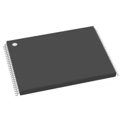
圖片僅供參考
XC5VLX85-1FFG676C
IC FPGA 440 I/O 676FCBGA
- 製造商
- 製造商。 部分 #XC5VLX85-1FFG676C
- 包 676-BBGA, FCBGA
- 資料表
- 有現貨的3397
100%原創; 新
24小時準備發貨
365天保修
RFQ&; 獲得更多折扣
規格
| Supplier | AMD Xilinx |
| Package | Tray |
| Series | Virtex®-5 LX |
| ProductStatus | Active |
| NumberofLABs/CLBs | 6480 |
| NumberofLogicElements/Cells | 82944 |
| TotalRAMBits | 3538944 |
| NumberofI/O | 440 |
| Voltage-Supply | 0.95V ~ 1.05V |
| MountingType | Surface Mount |
| OperatingTemperature | 0°C ~ 85°C (TJ) |
| Package/Case | 676-BBGA, FCBGA |
概述
Description
XC5VLX85-1FFG676C is a Xilinx Virtex-5 LX FPGA. It is a mid-to-high‑end 65 nm device designed for high‑performance logic, DSP, and embedded memory in a compact package. Key points:
- Package: 676‑pin FFG676, flip‑chip ball-grid array
- Temperature: Commercial (C) range
- Speed grade: -1 (fastest in the LX85 family)
- Resources (high level): thousands of configurable logic cells, DSP slices (DSP48E), block RAM, and multiple I/O banks with support for high‑speed I/O
- Serial I/O: capability for high‑speed transceivers; suitable for telecom, video processing, networking, and custom accelerator designs
- Tools: typically developed with Xilinx ISE Design Suite (legacy) and associated flow tools
In short, XC5VLX85-1FFG676C is a mid/high‑end Virtex‑5 FPGA option for complex, DSP‑heavy, I/O‑rich designs in a 676‑pin package.
Features
XC5VLX85-1FFG676C features (concise):
- Virtex-5 LX architecture with ~85k logic cells
- Speed grade -1 (fastest)
- 676‑pin FineLine BGA package (FFG676C)
- Multi-bank I/O with support for common LVTTL/LVCMOS and differential I/O standards
- On‑chip memory: Block RAM plus distributed RAM
- DSP capabilities: DSP slices for high‑speed MAC operations
- Clock management: PLLs and clock‑definition resources for multiple domains
- Flexible fabric for routing, LUTs, and logic reuse
- Configuration/JTAG for programming and debugging
- Power/area efficiency features typical of Virtex‑5 devices
Note: exact RAM/DSP counts and available I/O specifics vary by device variant; consult the datasheet for precise numbers.
Package
XC5VLX85-1FFG676C uses an FFG676 package—a Fine-Pitch Flip-Chip Ball Grid Array with 676 balls; temperature grade Commercial (C).
Pinout
- Pin count: 676 pins (FFG676 package)
- Function: Xilinx Virtex‑5 LX family FPGA (XC5VLX85) – a programmable logic device with DSP slices, Block RAM, configurable I/O and high-speed transceivers for digital designs.
- Function: Xilinx Virtex‑5 LX family FPGA (XC5VLX85) – a programmable logic device with DSP slices, Block RAM, configurable I/O and high-speed transceivers for digital designs.
Manufacturer
- Manufacturer: Xilinx, Inc. (now part of AMD)
- What kind of company: A semiconductor company specializing in programmable logic devices, primarily FPGAs and related design software.
- What kind of company: A semiconductor company specializing in programmable logic devices, primarily FPGAs and related design software.
Application
Typical applications for XC5VLX85-1FFG676C:
- High-performance DSP and signal-processing accelerators
- High-speed networking and telecom equipment (PCIe, Gigabit Ethernet, Serial RapidIO, SONET/SDH)
- Radar/sonar, wireless infrastructure and base stations
- Video, image processing and medical imaging
- Industrial control, data acquisition, and aerospace/defense systems
- Test & measurement and embedded processing platforms
船舶
運輸管道我們
通過DHL、FedEx、TNT、UPS或您選擇的任何其他貨運代理提供全球運輸服務。
運費參攷(DHL/FedEx):
動態主要裝載: 運費從25美元到45美元(0.5公斤)不等,預計交貨時間為2-5個工作日。
聯邦快遞: 運費從25美元到40美元(0.5公斤)不等,預計交貨時間為3-7個工作日。
不斷電供應系統: 運費從25美元到45美元(0.5公斤)不等,預計交貨時間為3-7個工作日。
三硝基甲苯: 運費從25美元到65美元(0.5公斤)不等,預計交貨時間為3-7個工作日。
增强型短消息: 運費從30美元到50美元(0.5公斤)不等,預計交貨時間為7-15個工作日。
掛號: 運費為2-4美元(0.1公斤),預計交貨時間為5-20個工作日。
支付
Payment Methods
付款條件為100%預付。
現時,我們只接受以下付款方式:
1. 貝寶
2. 信用卡/借記卡
3. 電匯
類似的
-
![MX25L3233FM1I-08Q]() MX25L3233FM1I-08Q
Macronix
-
![MX25V5126FM1I]() MX25V5126FM1I
Macronix
-
![MX25V4035FZUI]() MX25V4035FZUI
Macronix
-
![MX25V16066M1I02]() MX25V16066M1I02
Macronix
-
![MX25R3235FZNIL0]() MX25R3235FZNIL0
Macronix
-
![MX25L25673GMI-10G]() MX25L25673GMI-10G
Macronix
-
![MX25V1635FM2I]() MX25V1635FM2I
Macronix
-
![MX25U3232FZBI02]() MX25U3232FZBI02
Macronix
-
![MX25U6435FM2I-10G]() MX25U6435FM2I-10G
Macronix
-
![MX25L12833FM2I-10G]() MX25L12833FM2I-10..
Macronix
-
![MX25L12835FZ2I-10G]() MX25L12835FZ2I-10..
Macronix
-
![MX29LV160DTTI-70G]() MX29LV160DTTI-70G
Macronix