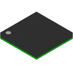
圖片僅供參考
XC2VP20-6FF896C
IC FPGA 556 I/O 896FCBGA
- 製造商
- 製造商。 部分 #XC2VP20-6FF896C
- 包
- 資料表 XC2VP20-6FF896C DataSheet
- 有現貨的8602
100%原創; 新
24小時準備發貨
365天保修
RFQ&; 獲得更多折扣
規格
| Series | Virtex®-II Pro |
| Part Status | Obsolete |
| DigiKey Programmable | Not Verified |
| Number of Logic Elements/Cells | 20880 |
| Total RAM Bits | 1622016 |
| Number of I/O | 556 |
| Voltage - Supply | 1.425V ~ 1.575V |
| Mounting Type | Surface Mount |
| Operating Temperature | 0°C ~ 85°C (TJ) |
| Package / Case | 896-BBGA, FCBGA |
| Supplier Device Package | 896-FCBGA (31x31) |
| Base Product Number | XC2VP20 |
| Number of LABs/CLBs | 2320 |
概述
Description
The XC2VP20-6FF896C is a model of FPGA (Field Programmable Gate Array) from Xilinx's Virtex-II Pro series. FPGAs are semiconductor devices that can be configured by the customer or designer after manufacturing, which allows for flexibility in implementing digital circuits.
The "XC2VP20" denotes the specific model within the Virtex-II Pro family, where "20" refers to its logic capacity. The "-6" indicates the speed grade, with lower numbers often representing faster performance. "FF896" refers to the package type and the number of pins; in this case, an 896-pin flip-chip fine-pitch BGA (Ball Grid Array) package is used.
This FPGA model features embedded PowerPC processor cores, making it suitable for high-performance applications that require both processing power and configurable logic. It includes a range of I/O capabilities, embedded multipliers, and block RAM, which are advantageous for applications in telecommunications, consumer electronics, and high-performance computing. The Virtex-II Pro series is known for its balance between logic resources, speed, and embedded processing capabilities.
The "XC2VP20" denotes the specific model within the Virtex-II Pro family, where "20" refers to its logic capacity. The "-6" indicates the speed grade, with lower numbers often representing faster performance. "FF896" refers to the package type and the number of pins; in this case, an 896-pin flip-chip fine-pitch BGA (Ball Grid Array) package is used.
This FPGA model features embedded PowerPC processor cores, making it suitable for high-performance applications that require both processing power and configurable logic. It includes a range of I/O capabilities, embedded multipliers, and block RAM, which are advantageous for applications in telecommunications, consumer electronics, and high-performance computing. The Virtex-II Pro series is known for its balance between logic resources, speed, and embedded processing capabilities.
Features
The XC2VP20-6FF896C is part of the Xilinx Virtex-II Pro FPGA family. Key features include:
1. Logic Resources: It contains about 20,088 logic cells, suitable for complex digital circuit designs.
2. Embedded PowerPC Processors: It features two embedded PowerPC 405 processor cores, which can be used for embedded processing applications.
3. I/O and Connectivity: It supports a range of I/O standards and features 556 user I/Os, making it versatile for various applications.
4. Memory: The FPGA includes Block RAM (BRAM) providing embedded memory for efficient data storage.
5. Clock Management: It offers advanced clock management capabilities, including Digital Clock Managers (DCMs) for precise clock signal control.
6. Speed Grade: The "-6" speed grade indicates a moderate level of performance in terms of timing and speed.
7. Package: The FF896 package denotes the physical layout and pin configuration, which is a Fine-Pitch Ball Grid Array (FBGA) with 896 pins.
These features make the XC2VP20-6FF896C suitable for applications in telecommunications, data processing, and embedded systems, where high performance and flexibility are required.
1. Logic Resources: It contains about 20,088 logic cells, suitable for complex digital circuit designs.
2. Embedded PowerPC Processors: It features two embedded PowerPC 405 processor cores, which can be used for embedded processing applications.
3. I/O and Connectivity: It supports a range of I/O standards and features 556 user I/Os, making it versatile for various applications.
4. Memory: The FPGA includes Block RAM (BRAM) providing embedded memory for efficient data storage.
5. Clock Management: It offers advanced clock management capabilities, including Digital Clock Managers (DCMs) for precise clock signal control.
6. Speed Grade: The "-6" speed grade indicates a moderate level of performance in terms of timing and speed.
7. Package: The FF896 package denotes the physical layout and pin configuration, which is a Fine-Pitch Ball Grid Array (FBGA) with 896 pins.
These features make the XC2VP20-6FF896C suitable for applications in telecommunications, data processing, and embedded systems, where high performance and flexibility are required.
Package
The XC2VP20-6FF896C is a Field-Programmable Gate Array (FPGA) from Xilinx's Virtex-II Pro family. It comes in an FF896 package type, which is a Flip-Chip Ball Grid Array (FCBGA) with 896 solder balls.
Pinout
The XC2VP20-6FF896C is a member of the Xilinx Virtex-II Pro family of FPGAs. It comes in an FF896 package, which indicates a Fine-Pitch Ball Grid Array (FBGA) with 896 pins. The XC2VP20 variant generally features embedded PowerPC processor cores, high-speed serial connectivity, and abundant logic resources suitable for a variety of applications.
The 896 pins are utilized for various functions, including:
1. User I/O: Provides input/output pins for interfacing with external devices.
2. Power and Ground: Supplies the necessary power (VCC, VCCO) and ensures stable operation.
3. Configuration: Supports modes for programming the FPGA (e.g., JTAG, SelectMAP).
4. Clocking: Includes dedicated clock pins for system synchronization.
5. Special Features: Pins for dedicated functionalities like high-speed serial links and memory interfaces.
The XC2VP20-6FF896C is suitable for applications requiring high performance, such as digital signal processing, embedded systems, and high-bandwidth data transfer.
The 896 pins are utilized for various functions, including:
1. User I/O: Provides input/output pins for interfacing with external devices.
2. Power and Ground: Supplies the necessary power (VCC, VCCO) and ensures stable operation.
3. Configuration: Supports modes for programming the FPGA (e.g., JTAG, SelectMAP).
4. Clocking: Includes dedicated clock pins for system synchronization.
5. Special Features: Pins for dedicated functionalities like high-speed serial links and memory interfaces.
The XC2VP20-6FF896C is suitable for applications requiring high performance, such as digital signal processing, embedded systems, and high-bandwidth data transfer.
Manufacturer
The XC2VP20-6FF896C is manufactured by Xilinx, which is a company specializing in the design and production of programmable logic devices. Xilinx is known for its FPGA (Field-Programmable Gate Array) products, which are used in a wide range of applications, including telecommunications, automotive, industrial, and consumer electronics. The company enables designers to configure custom hardware solutions, allowing for flexibility and adaptability in electronic designs. Xilinx was acquired by AMD in 2022, expanding AMD's portfolio in adaptive computing.
Application
The XC2VP20-6FF896C is a Virtex-II Pro FPGA from Xilinx, commonly used in high-performance applications such as digital signal processing, embedded systems, telecommunications, and networking. It is suitable for applications that require high-speed data processing and custom logic implementations, including video processing, wireless communication systems, and rapid prototyping of complex digital systems. Its embedded PowerPC processors and abundant I/O features make it ideal for applications demanding integrated processing capabilities and flexible interfacing options.
Equivalent
The XC2VP20-6FF896C is a member of Xilinx's Virtex-II Pro FPGA family. Equivalent products in terms of functionality and capacity could include other Xilinx FPGAs like certain models from the Virtex-4 series (e.g., XC4VLX25) or the Virtex-5 series (e.g., XC5VLX30). Competitors like Altera (now Intel) also offer similar FPGAs, such as those from the Stratix series. When selecting an equivalent, consider factors like logic cells, I/O pins, and specific application requirements.
船舶
運輸管道我們
通過DHL、FedEx、TNT、UPS或您選擇的任何其他貨運代理提供全球運輸服務。
運費參攷(DHL/FedEx):
動態主要裝載: 運費從25美元到45美元(0.5公斤)不等,預計交貨時間為2-5個工作日。
聯邦快遞: 運費從25美元到40美元(0.5公斤)不等,預計交貨時間為3-7個工作日。
不斷電供應系統: 運費從25美元到45美元(0.5公斤)不等,預計交貨時間為3-7個工作日。
三硝基甲苯: 運費從25美元到65美元(0.5公斤)不等,預計交貨時間為3-7個工作日。
增强型短消息: 運費從30美元到50美元(0.5公斤)不等,預計交貨時間為7-15個工作日。
掛號: 運費為2-4美元(0.1公斤),預計交貨時間為5-20個工作日。
支付
Payment Methods
付款條件為100%預付。
現時,我們只接受以下付款方式:
1. 貝寶
2. 信用卡/借記卡
3. 電匯
類似的
-
![MX30LF2G28AD-TI]() MX30LF2G28AD-TI
MX30LF2G28AD-TI
Macronix
-
![MX25R6435FBDIL0]() MX25R6435FBDIL0
MX25R6435FBDIL0
Macronix
-
![MX29GL512FHXFI-11G]() MX29GL512FHXFI-11..
MX29GL512FHXFI-11..
Macronix
-
![MX25U51279GXDR00]() MX25U51279GXDR00
MX25U51279GXDR00
Macronix
-
![MX25U25643GZNI00]() MX25U25643GZNI00
MX25U25643GZNI00
Macronix
-
![MX25L2006EM1I-12G]() MX25L2006EM1I-12G
MX25L2006EM1I-12G
Macronix
-
![MX25R1635FZUIH0]() MX25R1635FZUIH0
MX25R1635FZUIH0
Macronix
-
![MX25V1635FM2I]() MX25V1635FM2I
MX25V1635FM2I
Macronix
-
![MX25L12833FM2I-10G]() MX25L12833FM2I-10..
MX25L12833FM2I-10..
Macronix
-
![MX25L12833FZNI-10G]() MX25L12833FZNI-10..
MX25L12833FZNI-10..
Macronix
-
![MX25L12835FZ2I-10G]() MX25L12835FZ2I-10..
MX25L12835FZ2I-10..
Macronix
-
![MX29LV160DTTI-70G]() MX29LV160DTTI-70G
MX29LV160DTTI-70G
Macronix