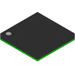
圖片僅供參考
W972GG6JB-25
IC DRAM 2GBIT PARALLEL 84WBGA
- 製造商
- 製造商。 部分 #W972GG6JB-25
- 包 84-TFBGA
- 資料表 W972GG6JB-25 DataSheet
- 有現貨的5764
100%原創; 新
24小時準備發貨
365天保修
RFQ&; 獲得更多折扣
規格
| Package | Tray |
| ProductStatus | Obsolete |
| MemoryType | Volatile |
| MemoryFormat | DRAM |
| Technology | SDRAM - DDR2 |
| MemorySize | 2Gb (128M x 16) |
| MemoryInterface | Parallel |
| ClockFrequency | 200 MHz |
| WriteCycleTime-WordPage | 15ns |
| AccessTime | 400 ps |
| Voltage-Supply | 1.7V ~ 1.9V |
| OperatingTemperature | 0°C ~ 85°C (TC) |
| MountingType | Surface Mount |
| Package/Case | 84-TFBGA |
概述
Description
W972GG6JB-25 is a specific model of DRAM (Dynamic Random Access Memory) produced by Winbond Electronics Corporation. It is designed for high-performance applications, often used in consumer electronics, computing devices, and embedded systems. This DRAM variant typically features a capacity of 2 Gigabits (Gb) and operates at a voltage of 1.8V, which is standard for low-power memory solutions.
The "25" in the model number often indicates a specific speed grade, suggesting it operates at a particular frequency, making it suitable for various applications that require efficient data processing. W972GG6JB-25 commonly employs a synchronous interface, ensuring reliable and fast data transfers.
Due to its specifications, this memory chip is particularly valued in scenarios where performance and energy efficiency are crucial, such as in mobile devices, automotive systems, and industrial applications. Understanding the characteristics of W972GG6JB-25 is essential for engineers and developers looking to optimize their designs for memory-intensive tasks.
The "25" in the model number often indicates a specific speed grade, suggesting it operates at a particular frequency, making it suitable for various applications that require efficient data processing. W972GG6JB-25 commonly employs a synchronous interface, ensuring reliable and fast data transfers.
Due to its specifications, this memory chip is particularly valued in scenarios where performance and energy efficiency are crucial, such as in mobile devices, automotive systems, and industrial applications. Understanding the characteristics of W972GG6JB-25 is essential for engineers and developers looking to optimize their designs for memory-intensive tasks.
Features
The W972GG6JB-25 is a DDR2 SDRAM memory chip from Winbond, featuring a density of 2Gb (Gigabits) and operating at a clock speed of 400 MHz. It supports a wide range of applications, including consumer electronics and computing devices. Key features include:
1. Data Rate: Offers a data rate of 800 MT/s (million transfers per second).
2. Organization: Configured as x16 or x8 for versatile integration.
3. Voltage: Operates at a low voltage of 1.8V, enhancing power efficiency.
4. Latency: Supports various CAS latency settings, contributing to flexible performance options.
5. Package: Available in a 60-ball TFBGA package, facilitating compact board designs.
6. Temperature Range: Designed for standard commercial temperature applications.
Overall, the W972GG6JB-25 combines high performance with energy efficiency, making it suitable for various consumer and industrial applications.
1. Data Rate: Offers a data rate of 800 MT/s (million transfers per second).
2. Organization: Configured as x16 or x8 for versatile integration.
3. Voltage: Operates at a low voltage of 1.8V, enhancing power efficiency.
4. Latency: Supports various CAS latency settings, contributing to flexible performance options.
5. Package: Available in a 60-ball TFBGA package, facilitating compact board designs.
6. Temperature Range: Designed for standard commercial temperature applications.
Overall, the W972GG6JB-25 combines high performance with energy efficiency, making it suitable for various consumer and industrial applications.
Package
The W972GG6JB-25 is a DRAM memory chip packaged in a standard FBGA (Fine Ball Grid Array) format.
Pinout
The W972GG6JB-25 is a 1Gb DDR2 SDRAM memory chip. It typically comes in a 60-ball FBGA (Fine Ball Grid Array) package.
The pin functions include:
1. Data Bus (DQ0-DQ63): 64 data lines for bi-directional data transfer.
2. Address Lines (A0-A12): Used to select memory addresses.
3. Control Signals (CS, RAS, CAS, WE): Control signals for chip selection, row address strobe, column address strobe, and write enable.
4. Clock (CLK): Provides timing for the memory operations.
5. Differential Clock (CKE): Enables and disables the device.
6. Bank Address (BA0-BA2): Selects bank addresses for memory operations.
7. Data Mask (DM): Used for write operations to mask data inputs.
This configuration allows the chip to support various memory operations efficiently in a DDR2 environment.
The pin functions include:
1. Data Bus (DQ0-DQ63): 64 data lines for bi-directional data transfer.
2. Address Lines (A0-A12): Used to select memory addresses.
3. Control Signals (CS, RAS, CAS, WE): Control signals for chip selection, row address strobe, column address strobe, and write enable.
4. Clock (CLK): Provides timing for the memory operations.
5. Differential Clock (CKE): Enables and disables the device.
6. Bank Address (BA0-BA2): Selects bank addresses for memory operations.
7. Data Mask (DM): Used for write operations to mask data inputs.
This configuration allows the chip to support various memory operations efficiently in a DDR2 environment.
Manufacturer
The W972GG6JB-25 is manufactured by Winbond Electronics Corporation, a Taiwanese semiconductor company. Founded in 1987, Winbond specializes in memory products, including DRAM (Dynamic Random Access Memory), Flash memory, and various semiconductor solutions. The company serves a wide range of applications, including consumer electronics, automotive, and industrial sectors. Winbond is known for its innovations in memory technology and is a key player in the global semiconductor market.
Application
The W972GG6JB-25 is a 1Gb DDR2 SDRAM memory chip commonly used in various application areas, including consumer electronics, computer systems, networking equipment, and telecommunications. It is suitable for use in laptops, desktops, servers, and embedded systems, providing high-speed data processing and efficient memory management in devices that require reliable performance and energy efficiency.
Equivalent
The W972GG6JB-25 chip, a 1Gb DDR2 SDRAM, has several equivalent products, including the following:
1. MT47H64M16HR-25
2. K4T1G164EB-25
3. Hynix H5TQ2G83AFR
4. Nanya NT5CB256M16DP-25
These alternatives should have similar specifications, including density, speed, and technology. Always verify compatibility based on the specific application requirements.
1. MT47H64M16HR-25
2. K4T1G164EB-25
3. Hynix H5TQ2G83AFR
4. Nanya NT5CB256M16DP-25
These alternatives should have similar specifications, including density, speed, and technology. Always verify compatibility based on the specific application requirements.
船舶
運輸管道我們
通過DHL、FedEx、TNT、UPS或您選擇的任何其他貨運代理提供全球運輸服務。
運費參攷(DHL/FedEx):
動態主要裝載: 運費從25美元到45美元(0.5公斤)不等,預計交貨時間為2-5個工作日。
聯邦快遞: 運費從25美元到40美元(0.5公斤)不等,預計交貨時間為3-7個工作日。
不斷電供應系統: 運費從25美元到45美元(0.5公斤)不等,預計交貨時間為3-7個工作日。
三硝基甲苯: 運費從25美元到65美元(0.5公斤)不等,預計交貨時間為3-7個工作日。
增强型短消息: 運費從30美元到50美元(0.5公斤)不等,預計交貨時間為7-15個工作日。
掛號: 運費為2-4美元(0.1公斤),預計交貨時間為5-20個工作日。
支付
Payment Methods
付款條件為100%預付。
現時,我們只接受以下付款方式:
1. 貝寶
2. 信用卡/借記卡
3. 電匯
類似的
-
![MX25L3233FZBI-08Q]() MX25L3233FZBI-08Q
MX25L3233FZBI-08Q
Macronix
-
![MX25L3233FM1I-08Q]() MX25L3233FM1I-08Q
MX25L3233FM1I-08Q
Macronix
-
![MX25V1635FZNQ03]() MX25V1635FZNQ03
MX25V1635FZNQ03
Macronix
-
![MX25V4035FZUI]() MX25V4035FZUI
MX25V4035FZUI
Macronix
-
![MX25R3235FZNIL0]() MX25R3235FZNIL0
MX25R3235FZNIL0
Macronix
-
![MX30LF2G28AD-TI]() MX30LF2G28AD-TI
MX30LF2G28AD-TI
Macronix
-
![MX29GL512FHXFI-11G]() MX29GL512FHXFI-11..
MX29GL512FHXFI-11..
Macronix
-
![MX25U25643GZNI00]() MX25U25643GZNI00
MX25U25643GZNI00
Macronix
-
![MX25R1635FZUIH0]() MX25R1635FZUIH0
MX25R1635FZUIH0
Macronix
-
![MX25U6435FM2I-10G]() MX25U6435FM2I-10G
MX25U6435FM2I-10G
Macronix
-
![MX25L12835FZ2I-10G]() MX25L12835FZ2I-10..
MX25L12835FZ2I-10..
Macronix
-
![MX29F040CTI-70G]() MX29F040CTI-70G
MX29F040CTI-70G
Macronix