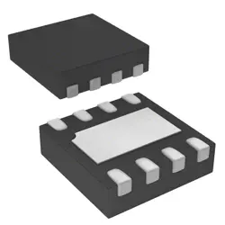
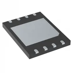
圖片僅供參考
TPS62067QDSGRQ1
IC REG BUCK ADJUSTABLE 2A 8WSON
- 製造商
- 製造商。 部分 #TPS62067QDSGRQ1
- 包 WSON-8
- 資料表
- 有現貨的3942
100%原創; 新
24小時準備發貨
365天保修
RFQ&; 獲得更多折扣
規格
| Package | Tape & Reel (TR),Cut Tape (CT) |
| Series | Automotive, AEC-Q100 |
| ProductStatus | Active |
| Function | Step-Down |
| OutputConfiguration | Positive |
| Topology | Buck |
| OutputType | Adjustable |
| NumberofOutputs | 1 |
| Voltage-Input(Min) | 2.9V |
| Voltage-Input(Max) | 6V |
| Voltage-Output(Min/Fixed) | 0.8V |
| Voltage-Output(Max) | 6V |
| Current-Output | 2A |
| Frequency-Switching | 3MHz |
| SynchronousRectifier | Yes |
| OperatingTemperature | -40°C ~ 125°C (TJ) |
| MountingType | Surface Mount |
| Package/Case | 8-WFDFN Exposed Pad |
概述
Description
The TPS62067QDSGRQ1 is a step-down (buck) DC-DC converter designed by Texas Instruments. It is part of their automotive-qualified product line, meeting AEC-Q100 standards, making it suitable for automotive and other high-reliability applications. The device operates with a wide input voltage range, typically from 2.3V to 6V, and delivers an adjustable output voltage down to 0.8V with a continuous output current of up to 2A.
Key features include high efficiency, achieved through its synchronous rectification topology, and a fast transient response supported by its DCS-Control™ architecture. The converter operates at a fixed frequency of 2.25 MHz, which helps reduce output ripple and allows for the use of smaller external components, thereby saving space on the PCB.
The TPS62067QDSGRQ1 also offers protection features such as overcurrent protection, thermal shutdown, and an undervoltage lockout. It supports power-save mode for improved efficiency at light loads and features a soft-start mechanism to limit inrush current during startup. The device is housed in a small 8-pin WSON package, making it suitable for compact designs.
Key features include high efficiency, achieved through its synchronous rectification topology, and a fast transient response supported by its DCS-Control™ architecture. The converter operates at a fixed frequency of 2.25 MHz, which helps reduce output ripple and allows for the use of smaller external components, thereby saving space on the PCB.
The TPS62067QDSGRQ1 also offers protection features such as overcurrent protection, thermal shutdown, and an undervoltage lockout. It supports power-save mode for improved efficiency at light loads and features a soft-start mechanism to limit inrush current during startup. The device is housed in a small 8-pin WSON package, making it suitable for compact designs.
Features
The TPS62067QDSGRQ1 is a high-efficiency step-down converter from Texas Instruments, designed primarily for automotive applications. Key features include:
1. Wide Input Voltage Range: Operates from 2.3V to 6V, making it suitable for a variety of power sources.
2. Output Current: Delivers up to 2A continuous output current, supporting a broad range of load requirements.
3. Efficiency: High efficiency typically up to 95%, achieved through the use of synchronous rectification.
4. Adjustable Output Voltage: Offers an adjustable output voltage, ranging from 0.8V to the input voltage.
5. Switching Frequency: Operates at a 2.4 MHz fixed switching frequency, allowing for smaller external components and a compact design.
6. Thermal Shutdown: Includes thermal shutdown protection to prevent damage due to overheating.
7. Automotive Qualified: AEC-Q100 qualified, ensuring reliability and performance in automotive environments.
8. Low Quiescent Current: Designed for low power consumption in non-switching mode, enhancing battery life.
These features make the TPS62067QDSGRQ1 suitable for applications that require high efficiency and compact size, such as infotainment systems, telematics, and advanced driver-assistance systems (ADAS).
1. Wide Input Voltage Range: Operates from 2.3V to 6V, making it suitable for a variety of power sources.
2. Output Current: Delivers up to 2A continuous output current, supporting a broad range of load requirements.
3. Efficiency: High efficiency typically up to 95%, achieved through the use of synchronous rectification.
4. Adjustable Output Voltage: Offers an adjustable output voltage, ranging from 0.8V to the input voltage.
5. Switching Frequency: Operates at a 2.4 MHz fixed switching frequency, allowing for smaller external components and a compact design.
6. Thermal Shutdown: Includes thermal shutdown protection to prevent damage due to overheating.
7. Automotive Qualified: AEC-Q100 qualified, ensuring reliability and performance in automotive environments.
8. Low Quiescent Current: Designed for low power consumption in non-switching mode, enhancing battery life.
These features make the TPS62067QDSGRQ1 suitable for applications that require high efficiency and compact size, such as infotainment systems, telematics, and advanced driver-assistance systems (ADAS).
Package
The TPS62067QDSGRQ1 is housed in a WSON (Wafer Level Chip Scale Package) with an 8-pin configuration. The specific package type is a 2 mm x 2 mm WSON, providing a compact design suitable for space-constrained applications.
Pinout
The TPS62067QDSGRQ1 is a step-down converter from Texas Instruments. It is designed for automotive applications and comes in an 8-pin WSON (DSG) package. Here’s a brief overview of its pin functions:
1. VIN: Input voltage supply pin where the input voltage is applied.
2. EN: Enable pin used to enable or disable the device. A high level enables the device, and a low level turns it off.
3. PG (Power Good): Open-drain output that indicates when the output voltage is within regulation.
4. SW: Switch pin connected to the internal MOSFET switch and inductor.
5. GND: Ground pin.
6. FB (Feedback): Feedback pin for connecting the output voltage to the internal error amplifier for regulation.
7. VOS: Output voltage sense pin, used to improve load regulation by sensing the output voltage.
8. SS/TR (Soft Start/Tracking): Allows for soft start or tracking of another voltage rail.
The TPS62067QDSGRQ1 is used for efficient power management with features like adjustable output voltage and high-frequency operation.
1. VIN: Input voltage supply pin where the input voltage is applied.
2. EN: Enable pin used to enable or disable the device. A high level enables the device, and a low level turns it off.
3. PG (Power Good): Open-drain output that indicates when the output voltage is within regulation.
4. SW: Switch pin connected to the internal MOSFET switch and inductor.
5. GND: Ground pin.
6. FB (Feedback): Feedback pin for connecting the output voltage to the internal error amplifier for regulation.
7. VOS: Output voltage sense pin, used to improve load regulation by sensing the output voltage.
8. SS/TR (Soft Start/Tracking): Allows for soft start or tracking of another voltage rail.
The TPS62067QDSGRQ1 is used for efficient power management with features like adjustable output voltage and high-frequency operation.
Manufacturer
The TPS62067QDSGRQ1 is manufactured by Texas Instruments (TI). Texas Instruments is a global semiconductor design and manufacturing company. It specializes in the production of analog and embedded processing chips, primarily serving industries such as automotive, industrial, personal electronics, communications equipment, and enterprise systems. TI is known for its broad range of integrated circuits and other semiconductor technologies that support a wide variety of electronic applications.
Application
The TPS62067QDSGRQ1 is a step-down converter designed for various applications requiring efficient power regulation. It is commonly used in automotive systems, battery-powered devices, industrial applications, and consumer electronics. Its compact size and high efficiency make it suitable for powering microcontrollers, sensors, and communication modules. Additionally, it is often utilized in infotainment systems and advanced driver-assistance systems (ADAS) in vehicles.
Equivalent
The TPS62067QDSGRQ1 is a step-down converter from Texas Instruments. Equivalent products include the LM3671 series from Texas Instruments, the LTC3621 from Analog Devices, the MP2145 from Monolithic Power Systems, and the MAX16974 from Maxim Integrated. These equivalents offer similar functionalities, such as voltage regulation, efficiency, and compact packaging, but you should verify specific parameters like output current, input voltage range, and efficiency to ensure compatibility with your application.
船舶
運輸管道我們
通過DHL、FedEx、TNT、UPS或您選擇的任何其他貨運代理提供全球運輸服務。
運費參攷(DHL/FedEx):
動態主要裝載: 運費從25美元到45美元(0.5公斤)不等,預計交貨時間為2-5個工作日。
聯邦快遞: 運費從25美元到40美元(0.5公斤)不等,預計交貨時間為3-7個工作日。
不斷電供應系統: 運費從25美元到45美元(0.5公斤)不等,預計交貨時間為3-7個工作日。
三硝基甲苯: 運費從25美元到65美元(0.5公斤)不等,預計交貨時間為3-7個工作日。
增强型短消息: 運費從30美元到50美元(0.5公斤)不等,預計交貨時間為7-15個工作日。
掛號: 運費為2-4美元(0.1公斤),預計交貨時間為5-20個工作日。
支付
Payment Methods
付款條件為100%預付。
現時,我們只接受以下付款方式:
1. 貝寶
2. 信用卡/借記卡
3. 電匯
類似的
-
![MX25L3233FZBI-08Q]() MX25L3233FZBI-08Q
MX25L3233FZBI-08Q
Macronix
-
![MX29F400CBTI-70G]() MX29F400CBTI-70G
MX29F400CBTI-70G
Macronix
-
![MX25V2033FM1I]() MX25V2033FM1I
MX25V2033FM1I
Macronix
-
![MX25V16066M1I02]() MX25V16066M1I02
MX25V16066M1I02
Macronix
-
![MX30LF2G28AD-TI]() MX30LF2G28AD-TI
MX30LF2G28AD-TI
Macronix
-
![MX25L8035EM2I-10G]() MX25L8035EM2I-10G
MX25L8035EM2I-10G
Macronix
-
![MX25L25673GMI-10G]() MX25L25673GMI-10G
MX25L25673GMI-10G
Macronix
-
![MX25R1635FZUIH0]() MX25R1635FZUIH0
MX25R1635FZUIH0
Macronix
-
![MX25L12833FM2I-10G]() MX25L12833FM2I-10..
MX25L12833FM2I-10..
Macronix
-
![MX25L12835FZ2I-10G]() MX25L12835FZ2I-10..
MX25L12835FZ2I-10..
Macronix
-
![MX29LV160DTTI-70G]() MX29LV160DTTI-70G
MX29LV160DTTI-70G
Macronix
-
![MX29F040CQI-70G]() MX29F040CQI-70G
MX29F040CQI-70G
Macronix