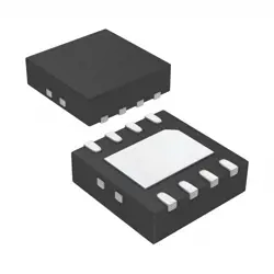
圖片僅供參考
TPS61040QDBVRQ1
IC LED DRVR RGLTR 400MA SOT23-5
- 製造商
- 製造商。 部分 #TPS61040QDBVRQ1
- 包 SOT-23-5
- 資料表
- 有現貨的5005
100%原創; 新
24小時準備發貨
365天保修
RFQ&; 獲得更多折扣
規格
| Package | Tape & Reel (TR),Cut Tape (CT) |
| Series | Automotive, AEC-Q100 |
| ProductStatus | Active |
| Type | DC DC Regulator |
| Topology | Step-Up (Boost) |
| InternalSwitch(s) | Yes |
| NumberofOutputs | 1 |
| Voltage-Supply(Min) | 1.8V |
| Voltage-Supply(Max) | 6V |
| Voltage-Output | 28V |
| Current-Output/Channel | 400mA (Switch) |
| Frequency | 1MHz |
| Applications | Backlight |
| OperatingTemperature | -40°C ~ 125°C (TJ) |
| MountingType | Surface Mount |
| Package/Case | SC-74A, SOT-753 |
概述
Description
The TPS61040QDBVRQ1 is a high-efficiency boost converter designed by Texas Instruments, tailored for automotive applications. It's part of the TPS61040-Q1 series, known for its compact size and efficiency. This device can convert input voltages ranging from 1.8V to 6V, making it suitable for battery-powered applications. It delivers an output voltage that can be set up to 28V, allowing flexibility in design.
A key feature of the TPS61040QDBVRQ1 is its ability to operate at a fixed switching frequency of 1.2 MHz, enabling the use of small external components and reducing overall system size. It also includes features such as a 400 mA switch current limit, thermal shutdown, and over-voltage protection to enhance reliability.
The device comes in a 5-pin SOT-23 package, which is ideal for space-constrained applications. Its automotive qualification (AEC-Q100) ensures that it meets the stringent requirements for automotive environments, including high-temperature operation and robust performance under various conditions, making it a reliable choice for boosting applications in automotive systems.
A key feature of the TPS61040QDBVRQ1 is its ability to operate at a fixed switching frequency of 1.2 MHz, enabling the use of small external components and reducing overall system size. It also includes features such as a 400 mA switch current limit, thermal shutdown, and over-voltage protection to enhance reliability.
The device comes in a 5-pin SOT-23 package, which is ideal for space-constrained applications. Its automotive qualification (AEC-Q100) ensures that it meets the stringent requirements for automotive environments, including high-temperature operation and robust performance under various conditions, making it a reliable choice for boosting applications in automotive systems.
Features
The TPS61040QDBVRQ1 is a high-efficiency, low-power boost converter designed for automotive applications. Key features include:
1. Wide Input Voltage Range: Operates from 1.8V to 6V, suitable for single-cell or dual-cell Alkaline/NiMH batteries and lithium-ion cells.
2. Adjustable Output Voltage: Capable of boosting output voltage up to 28V, configurable via external resistors.
3. High Efficiency: Up to 85% efficiency, with a switching frequency of 1.2 MHz, reducing the size of external components.
4. Low Quiescent Current: With a low 28 µA typical operating quiescent current, it extends battery life in portable applications.
5. Current Mode PWM Operation: Offers improved load and line regulation, ensuring stable performance across varying conditions.
6. Integrated Switch: Features a 400 mA switch, reducing the need for external components.
7. Protection Features: Includes over-temperature protection, over-current protection, and undervoltage lockout.
8. Automotive Grade: Qualified for automotive applications with an extended temperature range of –40°C to 125°C.
This device is ideal for applications requiring efficient high-voltage supply in compact, space-constrained environments.
1. Wide Input Voltage Range: Operates from 1.8V to 6V, suitable for single-cell or dual-cell Alkaline/NiMH batteries and lithium-ion cells.
2. Adjustable Output Voltage: Capable of boosting output voltage up to 28V, configurable via external resistors.
3. High Efficiency: Up to 85% efficiency, with a switching frequency of 1.2 MHz, reducing the size of external components.
4. Low Quiescent Current: With a low 28 µA typical operating quiescent current, it extends battery life in portable applications.
5. Current Mode PWM Operation: Offers improved load and line regulation, ensuring stable performance across varying conditions.
6. Integrated Switch: Features a 400 mA switch, reducing the need for external components.
7. Protection Features: Includes over-temperature protection, over-current protection, and undervoltage lockout.
8. Automotive Grade: Qualified for automotive applications with an extended temperature range of –40°C to 125°C.
This device is ideal for applications requiring efficient high-voltage supply in compact, space-constrained environments.
Package
The TPS61040QDBVRQ1 is typically provided in a SOT-23-6 package, which is a small, surface-mount package with six pins. This package is commonly used for compact electronic devices and circuits, offering a balance between size and thermal performance.
Pinout
The TPS61040QDBVRQ1 is a high-efficiency boost converter from Texas Instruments, designed for automotive applications. It comes in an SOT-23-6 package, which means it has 6 pins. Here are the functions of each pin:
1. SW (Switch): This pin is connected to the inductor and is the switch node of the boost converter.
2. GND (Ground): This is the ground reference for the device.
3. FB (Feedback): This pin is used to set the output voltage via an external resistor divider network.
4. EN (Enable): The enable pin is used to turn the device on or off. A high level enables the converter, while a low level disables it.
5. Vin (Input Voltage): This is the input supply voltage for the device.
6. Vout (Output Voltage): The output voltage is typically connected to an external LC filter to smooth out the voltage.
The TPS61040QDBVRQ1 is commonly used for boosting smaller input voltages to higher output voltages with high efficiency, suitable for automotive lighting and other electronic systems.
1. SW (Switch): This pin is connected to the inductor and is the switch node of the boost converter.
2. GND (Ground): This is the ground reference for the device.
3. FB (Feedback): This pin is used to set the output voltage via an external resistor divider network.
4. EN (Enable): The enable pin is used to turn the device on or off. A high level enables the converter, while a low level disables it.
5. Vin (Input Voltage): This is the input supply voltage for the device.
6. Vout (Output Voltage): The output voltage is typically connected to an external LC filter to smooth out the voltage.
The TPS61040QDBVRQ1 is commonly used for boosting smaller input voltages to higher output voltages with high efficiency, suitable for automotive lighting and other electronic systems.
Manufacturer
The TPS61040QDBVRQ1 is manufactured by Texas Instruments (TI). Texas Instruments is an American technology company that designs and manufactures semiconductors and various integrated circuits, which they sell to electronics designers and manufacturers globally. The company is known for its innovation in the fields of analog electronics, embedded processing, and digital signal processing. Texas Instruments serves a wide range of industries, including automotive, industrial, consumer electronics, and communications equipment. Their products are used in a variety of applications, from simple home electronics to complex industrial systems. The TPS61040QDBVRQ1 is a part of their portfolio of power management integrated circuits, specifically designed for boosting voltage in applications such as battery-powered devices.
Application
The TPS61040QDBVRQ1 is a high-efficiency boost converter designed for automotive applications. Its primary application areas include powering backlight displays, OLEDs, and other automotive electronic systems requiring voltage boosting from low-voltage sources. It is particularly suited for use in battery-powered devices where efficient power conversion is crucial.
Equivalent
The TPS61040QDBVRQ1 is a high-frequency boost converter from Texas Instruments. Equivalent products from other manufacturers include the LT1615 from Analog Devices, the NCP1400 from ON Semiconductor, and the MIC2287 from Microchip Technology. These components offer similar functionality for boosting voltage in low-power applications. Always compare the specific requirements of your application, such as output current, efficiency, and package type, when selecting an equivalent.
船舶
運輸管道我們
通過DHL、FedEx、TNT、UPS或您選擇的任何其他貨運代理提供全球運輸服務。
運費參攷(DHL/FedEx):
動態主要裝載: 運費從25美元到45美元(0.5公斤)不等,預計交貨時間為2-5個工作日。
聯邦快遞: 運費從25美元到40美元(0.5公斤)不等,預計交貨時間為3-7個工作日。
不斷電供應系統: 運費從25美元到45美元(0.5公斤)不等,預計交貨時間為3-7個工作日。
三硝基甲苯: 運費從25美元到65美元(0.5公斤)不等,預計交貨時間為3-7個工作日。
增强型短消息: 運費從30美元到50美元(0.5公斤)不等,預計交貨時間為7-15個工作日。
掛號: 運費為2-4美元(0.1公斤),預計交貨時間為5-20個工作日。
支付
Payment Methods
付款條件為100%預付。
現時,我們只接受以下付款方式:
1. 貝寶
2. 信用卡/借記卡
3. 電匯
類似的
-
![MX29F400CBTI-70G]() MX29F400CBTI-70G
MX29F400CBTI-70G
Macronix
-
![MX25V16066M1I02]() MX25V16066M1I02
MX25V16066M1I02
Macronix
-
![MX25R3235FZNIL0]() MX25R3235FZNIL0
MX25R3235FZNIL0
Macronix
-
![MX25V16066M2I02]() MX25V16066M2I02
MX25V16066M2I02
Macronix
-
![MX30LF2G28AD-TI]() MX30LF2G28AD-TI
MX30LF2G28AD-TI
Macronix
-
![MX25L8035EM2I-10G]() MX25L8035EM2I-10G
MX25L8035EM2I-10G
Macronix
-
![MX25R6435FBDIL0]() MX25R6435FBDIL0
MX25R6435FBDIL0
Macronix
-
![MX25L25673GMI-08G]() MX25L25673GMI-08G
MX25L25673GMI-08G
Macronix
-
![MX25L25673GMI-10G]() MX25L25673GMI-10G
MX25L25673GMI-10G
Macronix
-
![MX25L12833FM2I-10G]() MX25L12833FM2I-10..
MX25L12833FM2I-10..
Macronix
-
![MX25L12833FZNI-10G]() MX25L12833FZNI-10..
MX25L12833FZNI-10..
Macronix
-
![MX29LV160DTTI-70G]() MX29LV160DTTI-70G
MX29LV160DTTI-70G
Macronix