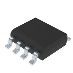
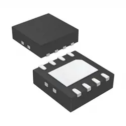
圖片僅供參考
TPS60150DRVR
IC REG CHARGE PUMP 5V 140MA 6SON
- 製造商
- 製造商。 部分 #TPS60150DRVR
- 包 WSON (DRV)-6
- 資料表
- 有現貨的3037
100%原創; 新
24小時準備發貨
365天保修
RFQ&; 獲得更多折扣
規格
| Package | Tape & Reel (TR),Cut Tape (CT),Bulk |
| ProductStatus | Active |
| Function | Step-Up |
| OutputConfiguration | Positive |
| Topology | Charge Pump |
| OutputType | Fixed |
| NumberofOutputs | 1 |
| Voltage-Input(Min) | 2.7V |
| Voltage-Input(Max) | 5.5V |
| Voltage-Output(Min/Fixed) | 5V |
| Current-Output | 140mA |
| Frequency-Switching | 1.5MHz |
| SynchronousRectifier | No |
| OperatingTemperature | -40°C ~ 85°C (TA) |
| MountingType | Surface Mount |
| Package/Case | 6-WDFN Exposed Pad |
概述
Description
The TPS60150DRVR is a step-up charge pump DC-DC converter designed by Texas Instruments. Optimized for efficiency and compactness, it is primarily used to generate higher output voltages from lower input voltages without requiring inductors, making it ideal for space-constrained applications. The device operates with a 1.8V to 3.6V input voltage range and can deliver a fixed output voltage of 3.3V or an adjustable output voltage up to 5.5V, making it suitable for powering microcontrollers, sensors, and other low-power devices.
Its key features include a high efficiency of up to 90%, low quiescent current, and the ability to handle a maximum output current of 150mA. The TPS60150DRVR also integrates short-circuit protection and thermal shutdown for enhanced reliability. Packaged in a small-footprint, 10-pin WSON (DRC) package, it is ideal for portable and battery-powered applications where board space is limited. The device's simple design, requiring few external components, and its ability to maintain high efficiency across a wide range of conditions make it a versatile choice for designers looking to implement step-up voltage conversion without the complexity of inductors.
Its key features include a high efficiency of up to 90%, low quiescent current, and the ability to handle a maximum output current of 150mA. The TPS60150DRVR also integrates short-circuit protection and thermal shutdown for enhanced reliability. Packaged in a small-footprint, 10-pin WSON (DRC) package, it is ideal for portable and battery-powered applications where board space is limited. The device's simple design, requiring few external components, and its ability to maintain high efficiency across a wide range of conditions make it a versatile choice for designers looking to implement step-up voltage conversion without the complexity of inductors.
Features
The TPS60150DRVR is a regulated charge pump voltage doubler designed for efficiency and compactness, ideal for applications requiring a stable output voltage. Key features include:
1. Input Voltage Range: Operates over a wide input voltage range, typically from 2.7V to 5.5V, making it versatile for various power sources.
2. Output Voltage: Provides a fixed output voltage up to 5V, suitable for powering portable devices.
3. Efficiency: High-efficiency operation, typically over 90%, which extends battery life in portable applications.
4. Regulation: The device includes internal regulation to maintain a constant output voltage over varying load conditions.
5. Low Quiescent Current: Offers low quiescent current, ensuring minimal power consumption in no-load or light-load scenarios.
6. Protection Features: Includes built-in protection features such as thermal shutdown and short-circuit protection to enhance reliability and safety.
7. Package: Available in a space-saving, thermally enhanced 10-pin DRV (WSON) package, suitable for compact designs.
This combination of features makes the TPS60150DRVR ideal for battery-powered applications where both efficiency and space are critical considerations.
1. Input Voltage Range: Operates over a wide input voltage range, typically from 2.7V to 5.5V, making it versatile for various power sources.
2. Output Voltage: Provides a fixed output voltage up to 5V, suitable for powering portable devices.
3. Efficiency: High-efficiency operation, typically over 90%, which extends battery life in portable applications.
4. Regulation: The device includes internal regulation to maintain a constant output voltage over varying load conditions.
5. Low Quiescent Current: Offers low quiescent current, ensuring minimal power consumption in no-load or light-load scenarios.
6. Protection Features: Includes built-in protection features such as thermal shutdown and short-circuit protection to enhance reliability and safety.
7. Package: Available in a space-saving, thermally enhanced 10-pin DRV (WSON) package, suitable for compact designs.
This combination of features makes the TPS60150DRVR ideal for battery-powered applications where both efficiency and space are critical considerations.
Package
The TPS60150DRVR is a Texas Instruments voltage regulator that comes in a WSON (VSON) package type, specifically a 10-pin DRV package. This package is compact, thermally efficient, and suitable for space-constrained applications.
Pinout
The TPS60150DRVR is a DC-DC charge pump voltage converter designed by Texas Instruments. It typically comes in a 10-pin WSON (DRC) package. Here's a brief overview of its pin functions:
1. VIN: Input voltage supply pin.
2. GND: Ground connection.
3. EN: Enable pin to turn the device on or off.
4. OUT: Output voltage pin.
5. C1+: Positive terminal for the external flying capacitor.
6. C1-: Negative terminal for the external flying capacitor.
7. C2+: Positive terminal for the second external flying capacitor.
8. C2-: Negative terminal for the second external flying capacitor.
9. FB: Feedback pin for output voltage regulation.
10. PGND: Power ground pin.
These pins work together to allow the TPS60150DRVR to efficiently boost voltage for various applications, such as powering OLED displays or other low-power devices requiring a regulated higher voltage output from a lower voltage input.
1. VIN: Input voltage supply pin.
2. GND: Ground connection.
3. EN: Enable pin to turn the device on or off.
4. OUT: Output voltage pin.
5. C1+: Positive terminal for the external flying capacitor.
6. C1-: Negative terminal for the external flying capacitor.
7. C2+: Positive terminal for the second external flying capacitor.
8. C2-: Negative terminal for the second external flying capacitor.
9. FB: Feedback pin for output voltage regulation.
10. PGND: Power ground pin.
These pins work together to allow the TPS60150DRVR to efficiently boost voltage for various applications, such as powering OLED displays or other low-power devices requiring a regulated higher voltage output from a lower voltage input.
Manufacturer
The TPS60150DRVR is manufactured by Texas Instruments Incorporated (TI). Texas Instruments is an American technology company that designs and manufactures semiconductors and various integrated circuits, which it sells to electronics designers and manufacturers globally. The company is a major player in the electronics industry and is known for its development of analog chips and embedded processors, which are crucial components in a wide range of electronic devices. TI's products are used in a variety of applications including industrial, automotive, personal electronics, and communications equipment.
Application
The TPS60150DRVR is a high-efficiency charge pump voltage inverter. Its application areas include powering negative voltage rails in industrial and consumer electronics, LCD display biasing, and powering operational amplifiers and other analog circuits. It is particularly useful in portable and battery-operated devices where efficient power management is crucial. Its compact size makes it suitable for space-constrained applications.
Equivalent
The TPS60150DRVR is a step-up charge pump voltage regulator by Texas Instruments. Equivalent products may include:
1. LM2750 by Texas Instruments
2. MAX1682 / MAX1683 by Maxim Integrated (now part of Analog Devices)
3. LTC1754 series by Analog Devices
4. MCP1252 by Microchip Technology
When selecting an equivalent, consider parameters like input/output voltage range, current rating, efficiency, and package type to ensure compatibility with your application.
1. LM2750 by Texas Instruments
2. MAX1682 / MAX1683 by Maxim Integrated (now part of Analog Devices)
3. LTC1754 series by Analog Devices
4. MCP1252 by Microchip Technology
When selecting an equivalent, consider parameters like input/output voltage range, current rating, efficiency, and package type to ensure compatibility with your application.
船舶
運輸管道我們
通過DHL、FedEx、TNT、UPS或您選擇的任何其他貨運代理提供全球運輸服務。
運費參攷(DHL/FedEx):
動態主要裝載: 運費從25美元到45美元(0.5公斤)不等,預計交貨時間為2-5個工作日。
聯邦快遞: 運費從25美元到40美元(0.5公斤)不等,預計交貨時間為3-7個工作日。
不斷電供應系統: 運費從25美元到45美元(0.5公斤)不等,預計交貨時間為3-7個工作日。
三硝基甲苯: 運費從25美元到65美元(0.5公斤)不等,預計交貨時間為3-7個工作日。
增强型短消息: 運費從30美元到50美元(0.5公斤)不等,預計交貨時間為7-15個工作日。
掛號: 運費為2-4美元(0.1公斤),預計交貨時間為5-20個工作日。
支付
Payment Methods
付款條件為100%預付。
現時,我們只接受以下付款方式:
1. 貝寶
2. 信用卡/借記卡
3. 電匯
類似的
-
![MX25L3233FZBI-08Q]() MX25L3233FZBI-08Q
MX25L3233FZBI-08Q
Macronix
-
![MX25V1635FZNI]() MX25V1635FZNI
MX25V1635FZNI
Macronix
-
![MX29F400CBTI-70G]() MX29F400CBTI-70G
MX29F400CBTI-70G
Macronix
-
![MX25V5126FM1I]() MX25V5126FM1I
MX25V5126FM1I
Macronix
-
![MX25V4035FZUI]() MX25V4035FZUI
MX25V4035FZUI
Macronix
-
![MX25L25673GMI-08G]() MX25L25673GMI-08G
MX25L25673GMI-08G
Macronix
-
![MX25U51279GXDR00]() MX25U51279GXDR00
MX25U51279GXDR00
Macronix
-
![MX25U25643GZNI00]() MX25U25643GZNI00
MX25U25643GZNI00
Macronix
-
![MX25V1635FM2I]() MX25V1635FM2I
MX25V1635FM2I
Macronix
-
![MX25L12833FZNI-10G]() MX25L12833FZNI-10..
MX25L12833FZNI-10..
Macronix
-
![MX25U25645GXDI00]() MX25U25645GXDI00
MX25U25645GXDI00
Macronix
-
![MX25L25645GXDI-08G]() MX25L25645GXDI-08..
MX25L25645GXDI-08..
Macronix