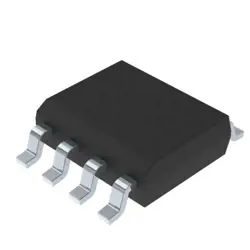
圖片僅供參考
TNY264GN
IC OFFLINE SWITCH FLYBACK 8SMD
- 製造商
- 製造商。 部分 #TNY264GN
- 包 SMD-8
- 資料表
- 有現貨的2072
100%原創; 新
24小時準備發貨
365天保修
RFQ&; 獲得更多折扣
規格
| Package | Tube |
| Series | TinySwitch®-II |
| ProductStatus | Discontinued at Digi-Key |
| OutputIsolation | Isolated |
| InternalSwitch(s) | Yes |
| Voltage-Breakdown | 700V |
| Topology | Flyback |
| DutyCycle | 65% |
| Frequency-Switching | 132kHz |
| Power(Watts) | 9 W |
| FaultProtection | Current Limiting, Open Loop, Over Temperature, Short Circuit |
| ControlFeatures | EN |
| OperatingTemperature | -40°C ~ 150°C (TJ) |
| Package/Case | 8-SMD (7 Leads), Gull Wing |
| SupplierDevicePackage | SMD-8B |
概述
Description
The TNY264GN is a member of the TinySwitch-II family of energy-efficient, off-line switcher ICs designed by Power Integrations. It is commonly used for power supply applications that require low standby power consumption and high efficiency. The TNY264GN integrates a 700V power MOSFET, oscillator, high-voltage switched current source, current limit, and thermal shutdown circuitry into a single IC, reducing the number of components needed for a power supply design.
Key features include auto-restart for short circuit and open loop protection, frequency jittering to reduce EMI, and under-voltage and over-voltage protection. The IC supports a power range suitable for adapters, chargers, and standby supplies, typically up to 10W. Its compact design allows for a smaller overall footprint, while the integrated features simplify the design process and improve reliability. It is available in a surface-mount SMD package, making it suitable for modern manufacturing processes. Overall, the TNY264GN is valued for its ability to deliver efficient performance in compact power solutions.
Key features include auto-restart for short circuit and open loop protection, frequency jittering to reduce EMI, and under-voltage and over-voltage protection. The IC supports a power range suitable for adapters, chargers, and standby supplies, typically up to 10W. Its compact design allows for a smaller overall footprint, while the integrated features simplify the design process and improve reliability. It is available in a surface-mount SMD package, making it suitable for modern manufacturing processes. Overall, the TNY264GN is valued for its ability to deliver efficient performance in compact power solutions.
Features
The TNY264GN is a member of the TinySwitch-II family of integrated circuits, used primarily in power supply applications. Key features include:
1. Primary-Side Control: It integrates a 700 V power MOSFET, oscillator, high voltage switched current source, current limit, and thermal shutdown circuitry onto a single monolithic device.
2. Efficiency: Offers high efficiency with low standby power consumption, making it suitable for energy-efficient power supplies.
3. Cycle-by-Cycle Current Limiting: This feature provides enhanced overload protection.
4. Auto-Restart: In the event of a fault condition, the device automatically restarts, reducing component stress and power supply failures.
5. Built-in Frequency Jittering: Helps in reducing EMI, allowing for simpler filtering and compliance with global emission standards.
6. Thermal Shutdown Protection: Automatically shuts down the device when the junction temperature exceeds a certain limit, preventing damage from overheating.
7. Wide Input Voltage Range: Supports a wide operating range, making it versatile for various applications.
8. Low Component Count: Simplifies design, reducing overall system cost and size.
These features make the TNY264GN ideal for compact and efficient power supply designs in various consumer electronics and industrial applications.
1. Primary-Side Control: It integrates a 700 V power MOSFET, oscillator, high voltage switched current source, current limit, and thermal shutdown circuitry onto a single monolithic device.
2. Efficiency: Offers high efficiency with low standby power consumption, making it suitable for energy-efficient power supplies.
3. Cycle-by-Cycle Current Limiting: This feature provides enhanced overload protection.
4. Auto-Restart: In the event of a fault condition, the device automatically restarts, reducing component stress and power supply failures.
5. Built-in Frequency Jittering: Helps in reducing EMI, allowing for simpler filtering and compliance with global emission standards.
6. Thermal Shutdown Protection: Automatically shuts down the device when the junction temperature exceeds a certain limit, preventing damage from overheating.
7. Wide Input Voltage Range: Supports a wide operating range, making it versatile for various applications.
8. Low Component Count: Simplifies design, reducing overall system cost and size.
These features make the TNY264GN ideal for compact and efficient power supply designs in various consumer electronics and industrial applications.
Package
The TNY264GN is a power integration IC and comes in an 8-pin surface mount package known as SOIC-8 (Small Outline Integrated Circuit). This package type is commonly used for its compact size and reliability in electronic circuit designs.
Pinout
The TNY264GN is an integrated circuit from the TinySwitch-II family, designed for use in energy-efficient, low-power offline switcher applications. It typically comes in an 8-pin SOIC (Small Outline Integrated Circuit) package. The pin functions are as follows:
1. SOURCE (Pin 1, 2, 3, 8): These pins are internally connected in the IC and should be connected externally to the primary side of the transformer. They serve as the return path for the switching currents and provide heat dissipation.
2. BP (BYPASS) (Pin 4): This pin is connected to an external capacitor to provide a stable voltage reference for internal operations and to set the current limit programming.
3. DRAIN (Pin 5): This is the high voltage power MOSFET drain connection, which connects to the primary winding of the transformer.
4. ENABLE/UNDER-VOLTAGE (Pin 6): This pin enables the IC and provides under-voltage lockout, ensuring that the device operates only when the input voltage is above a certain threshold.
7. NC (Pin 7): This pin is typically not connected and is reserved for future use or internal purposes.
These pins help the TNY264GN function effectively in cost-sensitive and space-constrained power supply applications.
1. SOURCE (Pin 1, 2, 3, 8): These pins are internally connected in the IC and should be connected externally to the primary side of the transformer. They serve as the return path for the switching currents and provide heat dissipation.
2. BP (BYPASS) (Pin 4): This pin is connected to an external capacitor to provide a stable voltage reference for internal operations and to set the current limit programming.
3. DRAIN (Pin 5): This is the high voltage power MOSFET drain connection, which connects to the primary winding of the transformer.
4. ENABLE/UNDER-VOLTAGE (Pin 6): This pin enables the IC and provides under-voltage lockout, ensuring that the device operates only when the input voltage is above a certain threshold.
7. NC (Pin 7): This pin is typically not connected and is reserved for future use or internal purposes.
These pins help the TNY264GN function effectively in cost-sensitive and space-constrained power supply applications.
Manufacturer
The TNY264GN is manufactured by Power Integrations, Inc. Power Integrations is a semiconductor company that specializes in developing and producing high-performance electronic components used in high-voltage power conversion systems. Their products are widely used in various applications, including consumer electronics, industrial devices, and renewable energy systems, to enhance energy efficiency and reduce electronic waste. The company is known for its innovations in power supply design, particularly in integrating power conversion functions into a single chip.
Application
The TNY264GN is a TinySwitch-II series integrated circuit used in power supply applications. It is commonly used for off-line switcher solutions in power adapters, chargers, and auxiliary power supplies for appliances, industrial systems, and consumer electronics. Its features, like high efficiency and low standby power, make it suitable for compact and cost-effective designs in low-power applications, typically up to 15W.
Equivalent
The TNY264GN is a TinySwitch-II family integrated circuit used for energy-efficient power supply designs. Equivalent products include other members of the TinySwitch-II family, like TNY263GN, TNY265GN, and TNY266GN, which offer similar functionality with slight variations in power output or features. Additionally, other manufacturers may have equivalent products with similar specifications, such as ON Semiconductor's NCP1xx series or Fairchild's FSD series. Always verify the specific requirements and compatibility when selecting an equivalent.
船舶
運輸管道我們
通過DHL、FedEx、TNT、UPS或您選擇的任何其他貨運代理提供全球運輸服務。
運費參攷(DHL/FedEx):
動態主要裝載: 運費從25美元到45美元(0.5公斤)不等,預計交貨時間為2-5個工作日。
聯邦快遞: 運費從25美元到40美元(0.5公斤)不等,預計交貨時間為3-7個工作日。
不斷電供應系統: 運費從25美元到45美元(0.5公斤)不等,預計交貨時間為3-7個工作日。
三硝基甲苯: 運費從25美元到65美元(0.5公斤)不等,預計交貨時間為3-7個工作日。
增强型短消息: 運費從30美元到50美元(0.5公斤)不等,預計交貨時間為7-15個工作日。
掛號: 運費為2-4美元(0.1公斤),預計交貨時間為5-20個工作日。
支付
Payment Methods
付款條件為100%預付。
現時,我們只接受以下付款方式:
1. 貝寶
2. 信用卡/借記卡
3. 電匯
類似的
-
![MX25L3233FZBI-08Q]() MX25L3233FZBI-08Q
MX25L3233FZBI-08Q
Macronix
-
![MX25V1635FZNQ03]() MX25V1635FZNQ03
MX25V1635FZNQ03
Macronix
-
![MX29F400CBTI-70G]() MX29F400CBTI-70G
MX29F400CBTI-70G
Macronix
-
![MX25V4035FZUI]() MX25V4035FZUI
MX25V4035FZUI
Macronix
-
![MX25V16066M1I02]() MX25V16066M1I02
MX25V16066M1I02
Macronix
-
![MX25L8035EM2I-10G]() MX25L8035EM2I-10G
MX25L8035EM2I-10G
Macronix
-
![MX25L25673GMI-10G]() MX25L25673GMI-10G
MX25L25673GMI-10G
Macronix
-
![MX25V1635FM2I]() MX25V1635FM2I
MX25V1635FM2I
Macronix
-
![MX25L12833FM2I-10G]() MX25L12833FM2I-10..
MX25L12833FM2I-10..
Macronix
-
![MX25L12833FZ2I-10G]() MX25L12833FZ2I-10..
MX25L12833FZ2I-10..
Macronix
-
![MX25L12833FZNI-10G]() MX25L12833FZNI-10..
MX25L12833FZNI-10..
Macronix
-
![MX29LV160DTTI-70G]() MX29LV160DTTI-70G
MX29LV160DTTI-70G
Macronix