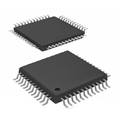
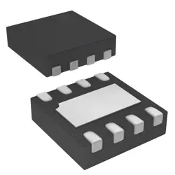
圖片僅供參考
SY89832UMG
IC CLK BUFFER 1:4 2.5GHZ 16MLF
- 製造商
- 製造商。 部分 #SY89832UMG
- 包
- 資料表 SY89832UMG DataSheet
- 有現貨的4207
100%原創; 新
24小時準備發貨
365天保修
RFQ&; 獲得更多折扣
規格
| Series | Precision Edge® |
| Part Status | Active |
| Base Product Number | SY89832 |
| Type | Fanout Buffer (Distribution), Translator |
| Number of Circuits | 1 |
| Ratio - Input:Output | 1:4 |
| Differential - Input:Output | Yes/Yes |
| Input | CML, LVDS, LVPECL |
| Output | LVDS |
| Frequency - Max | 2.5 GHz |
| Voltage - Supply | 2.375V ~ 2.625V |
| Operating Temperature | -40°C ~ 85°C |
| Mounting Type | Surface Mount |
| Package | 16-VFQFN Exposed Pad, 16-MLF® |
| Supplier Device Package | 16-MLF® (3x3) |
| Packaging | Tube |
概述
Description
The "Introduction to SY89832UMG" likely refers to a specific product, model, or technology designation, though it isn't immediately recognizable from publicly available information as of my last update. If SY89832UMG pertains to a recent technological product, semiconductor component, or specialized equipment, an introductory overview would typically cover its purpose, key features, and applications.
For instance, if SY89832UMG were a semiconductor or microcontroller, the introduction might highlight its role in electronic systems, such as enabling efficient data processing, supporting communication protocols, or enhancing device performance. Key features could include processing speed, power efficiency, integration capabilities, or compatibility with other technologies. The applications might range from consumer electronics and automotive systems to industrial automation and telecommunications.
For precise information, it would be best to consult the manufacturer's documentation or technical datasheets, which provide detailed specifications, usage guidelines, and support resources.
Features
The SY89832UMG is a precision, high-speed, low-jitter 1:2 differential fanout buffer often used in applications requiring clock distribution. Key features include:
1. High-Speed Operation: Typically supports data rates up to several gigahertz, making it suitable for high-frequency clock distribution.
2. Low Jitter: Designed to provide low phase noise and jitter, which is critical for maintaining signal integrity in high-speed applications.
3. Differential Inputs and Outputs: Utilizes differential signaling to enhance noise immunity and minimize signal distortion.
4. Output Fanout: Capable of driving multiple outputs from a single input, which is useful for distributing a clock signal to multiple devices.
5. Power Supply: Operates on a single power supply, typically in the range of 2.5V to 3.3V.
6. Package: Comes in a compact package, such as MSOP or similar, which is suitable for space-constrained applications.
7. Temperature Range: Supports a wide operating temperature range, often from -40°C to +85°C, making it suitable for industrial applications.
These features make the SY89832UMG a reliable choice for applications in networking, telecommunications, and other high-performance computing environments.
Package
The SY89832UMG is typically available in a Micro Leadframe Package (MLP), also known as a Micro Leadframe Package Quad Flat No-leads (MLP-QFN). This package type is known for its small size and efficient heat dissipation, making it suitable for high-density applications.
Pinout
The SY89832UMG is a high-speed, 2:1 multiplexer designed for high-performance networking and communications applications. It typically comes in an 8-pin Micro Leadframe Package (MLP) or MicroPak.
Here is a brief overview of its pin functions:
1. IN0, IN1: These are the differential inputs for the multiplexer.
2. /SEL: This is the select pin used to choose between IN0 and IN1. A low or high logic level here selects the respective input.
3. /OE: This is the output enable pin. When low, the output is enabled; when high, the output is in a high-impedance state.
4. Q, /Q: These are the differential outputs of the multiplexer.
5. VCC: This is the power supply pin.
6. GND: This is the ground pin, serving as the reference for the device.
The SY89832UMG offers low jitter and ensures signal integrity, making it suitable for critical applications requiring fast and reliable data transmission.
Manufacturer
The manufacturer of the SY89832UMG is Microchip Technology Inc. Microchip Technology is a leading provider of microcontroller, mixed-signal, analog, and Flash-IP solutions. The company focuses on delivering a wide range of semiconductor products for various applications, including automotive, industrial, consumer, aerospace, and data communications sectors. Microchip is known for its emphasis on providing comprehensive development tools, design resources, and customer support to facilitate the integration of their products into larger systems.
Application
The SY89832UMG is a high-speed differential receiver/driver commonly used in applications requiring precise timing and signal integrity. Its primary application areas include telecommunications, data communications, high-speed networking, and digital video systems. It is utilized in clock distribution, high-frequency signal processing, and interface conversion where reliable low-jitter signal transmission is critical.
Equivalent
The SY89832UMG is a high-speed differential LVPECL to LVPECL translator/multiplexer. Equivalent products might include:
1. On Semiconductor MC100EP56 - LVPECL Multiplexer with Similar Functionality
2. Texas Instruments CDCLVP1102 - Low Jitter LVPECL Buffer
3. Microchip Technology SY58031U - Ultra-Precision Differential LVPECL Multiplexer
Always verify pin compatibility and electrical specifications to ensure proper substitution.
船舶
運輸管道我們
通過DHL、FedEx、TNT、UPS或您選擇的任何其他貨運代理提供全球運輸服務。
運費參攷(DHL/FedEx):
動態主要裝載: 運費從25美元到45美元(0.5公斤)不等,預計交貨時間為2-5個工作日。
聯邦快遞: 運費從25美元到40美元(0.5公斤)不等,預計交貨時間為3-7個工作日。
不斷電供應系統: 運費從25美元到45美元(0.5公斤)不等,預計交貨時間為3-7個工作日。
三硝基甲苯: 運費從25美元到65美元(0.5公斤)不等,預計交貨時間為3-7個工作日。
增强型短消息: 運費從30美元到50美元(0.5公斤)不等,預計交貨時間為7-15個工作日。
掛號: 運費為2-4美元(0.1公斤),預計交貨時間為5-20個工作日。
支付
Payment Methods
付款條件為100%預付。
現時,我們只接受以下付款方式:
1. 貝寶
2. 信用卡/借記卡
3. 電匯
類似的
-
![MX25V1635FZNQ03]() MX25V1635FZNQ03
Macronix
-
![MX29F400CBTI-70G]() MX29F400CBTI-70G
Macronix
-
![MX66U1G45GXDI00]() MX66U1G45GXDI00
Macronix
-
![MX25V4035FZUI]() MX25V4035FZUI
Macronix
-
![MX25V16066M1I02]() MX25V16066M1I02
Macronix
-
![MX25V16066M2I02]() MX25V16066M2I02
Macronix
-
![MX25L8035EM2I-10G]() MX25L8035EM2I-10G
Macronix
-
![MX25L25673GMI-08G]() MX25L25673GMI-08G
Macronix
-
![MX25L25673GMI-10G]() MX25L25673GMI-10G
Macronix
-
![MX25U51279GXDR00]() MX25U51279GXDR00
Macronix
-
![MX25U25643GZNI00]() MX25U25643GZNI00
Macronix
-
![MX25U3232FZBI02]() MX25U3232FZBI02
Macronix