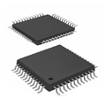
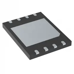
圖片僅供參考
STBP112CVDJ6F
IC OVP PROTECTION TDFN-8
- 製造商
- 製造商。 部分 #STBP112CVDJ6F
- 包 TDFN-8
- 資料表 STBP112CVDJ6F DataSheet
- 有現貨的4597
100%原創; 新
24小時準備發貨
365天保修
RFQ&; 獲得更多折扣
規格
| Package | Tape & Reel (TR),Cut Tape (CT) |
| ProductStatus | Active |
| Technology | Internal Switch |
| NumberofCircuits | 1 |
| Applications | General Purpose |
| MountingType | Surface Mount |
| Package/Case | 8-WFDFN Exposed Pad |
概述
Description
STBP112CVDJ6F is a specific part number that typically refers to a type of electronic component, possibly a semiconductor or integrated circuit. The name suggests it could be related to a specific functionality such as a voltage regulator, operational amplifier, or a similar device used in electronic applications.
To provide a precise introduction, it is essential to consult the manufacturer's datasheet or relevant technical documentation, which will detail its specifications, pin configuration, functionalities, applications, and electrical characteristics. If you're looking for more specific information or context regarding STBP112CVDJ6F, please provide more details or clarify the type of component you are interested in.
To provide a precise introduction, it is essential to consult the manufacturer's datasheet or relevant technical documentation, which will detail its specifications, pin configuration, functionalities, applications, and electrical characteristics. If you're looking for more specific information or context regarding STBP112CVDJ6F, please provide more details or clarify the type of component you are interested in.
Features
The STBP112CVDJ6F is a dual-channel power switch designed for controlling power to loads with high efficiency and reliability. Key features include:
1. Dual High-Side Switches: It integrates two independent switches, allowing for flexible load management.
2. Low On-Resistance: Offers a low on-resistance (typically around 30 mΩ), which minimizes power loss and heat generation.
3. Wide Supply Voltage Range: Operates within a range of 1.8V to 5.5V, accommodating various applications.
4. Fast Switching Times: Ensures quick response times for efficient operation.
5. Thermal and Overcurrent Protection: Includes features for enhanced reliability, protecting against overheating and overcurrent conditions.
6. Small Package Size: Available in a compact package (SOT-23), making it suitable for space-constrained applications.
7. Low Quiescent Current: Consumes minimal power in standby mode, enhancing energy efficiency.
These features make the STBP112CVDJ6F ideal for applications in portable devices, battery-powered equipment, and general power management.
Package
The STBP112CVDJ6F is packaged in a DPAK (TO-252) form factor. This surface-mount package is designed for power applications, offering a compact footprint and efficient thermal performance.
Pinout
The STBP112CVDJ6F is a dual-channel, high-speed, low-side N-channel MOSFET driver from STMicroelectronics. It features a 16-pin HTSSOP package.
The pin count is 16, with the following key functions:
1. IN_A, IN_B (Pins 1, 2): Input signals for channel A and B to control the MOSFETs.
2. OUT_A, OUT_B (Pins 3, 4): Output signals to drive the gates of the respective MOSFETs.
3. VSUP (Pin 5): Supply voltage input.
4. GND (Pin 6): Ground connection.
5. BOOT_A, BOOT_B (Pins 7, 8): Bootstrap capacitors for high-side MOSFET driving.
6. COMP_A, COMP_B (Pins 9, 10): Compensation pins for stability.
7. R_T (Pin 11): Timing resistor for adjustable delay.
8. VREG (Pin 12): Regulated output voltage for internal circuitry.
9. NC (Pins 13, 14, 15, 16): Not connected pins, typically used for thermal dissipation or reserved for future use.
This device is commonly used in applications like motor control, power management, and DC-DC converters.
Manufacturer
The STBP112CVDJ6F is manufactured by STMicroelectronics, a global semiconductor company headquartered in Geneva, Switzerland. STMicroelectronics specializes in the design and production of a wide range of semiconductor devices and technologies, including integrated circuits, microcontrollers, sensors, and power management solutions. The company serves various industries such as automotive, industrial, consumer electronics, and communications. With a strong focus on innovation and sustainability, STMicroelectronics plays a significant role in advancing technologies that support the Internet of Things (IoT), smart mobility, and energy efficiency.
Application
The STBP112CVDJ6F is a high-speed, dual-channel power switch designed for a range of applications, including power management in consumer electronics, battery-operated devices, USB interface power switching, and general load switching in industrial applications. Its low on-resistance and fast switching capabilities make it suitable for use in mobile devices, tablets, and portable gadgets where efficient power distribution is essential.
Equivalent
The STBP112CVDJ6F is a dual-channel high-speed low-side N-channel MOSFET driver. Equivalent products include the MIC4426, TC4420, and NCP81074. Always verify specifications such as gate drive voltage, current capacity, and package type to ensure compatibility.
船舶
運輸管道我們
通過DHL、FedEx、TNT、UPS或您選擇的任何其他貨運代理提供全球運輸服務。
運費參攷(DHL/FedEx):
動態主要裝載: 運費從25美元到45美元(0.5公斤)不等,預計交貨時間為2-5個工作日。
聯邦快遞: 運費從25美元到40美元(0.5公斤)不等,預計交貨時間為3-7個工作日。
不斷電供應系統: 運費從25美元到45美元(0.5公斤)不等,預計交貨時間為3-7個工作日。
三硝基甲苯: 運費從25美元到65美元(0.5公斤)不等,預計交貨時間為3-7個工作日。
增强型短消息: 運費從30美元到50美元(0.5公斤)不等,預計交貨時間為7-15個工作日。
掛號: 運費為2-4美元(0.1公斤),預計交貨時間為5-20個工作日。
支付
Payment Methods
付款條件為100%預付。
現時,我們只接受以下付款方式:
1. 貝寶
2. 信用卡/借記卡
3. 電匯
類似的
-
![MX25R8035FM1IL0]() MX25R8035FM1IL0
Macronix
-
![MX25L3233FZBI-08Q]() MX25L3233FZBI-08Q
Macronix
-
![MX25L3233FM1I-08Q]() MX25L3233FM1I-08Q
Macronix
-
![MX29F400CBTI-70G]() MX29F400CBTI-70G
Macronix
-
![MX66U1G45GXDI00]() MX66U1G45GXDI00
Macronix
-
![MX25V5126FM1I]() MX25V5126FM1I
Macronix
-
![MX30LF2G28AD-TI]() MX30LF2G28AD-TI
Macronix
-
![MX25L25673GMI-10G]() MX25L25673GMI-10G
Macronix
-
![MX25U51279GXDR00]() MX25U51279GXDR00
Macronix
-
![MX25L6433FM2I-08G]() MX25L6433FM2I-08G
Macronix
-
![MX25U6435FM2I-10G]() MX25U6435FM2I-10G
Macronix
-
![MX25L12833FZ2I-10G]() MX25L12833FZ2I-10..
Macronix