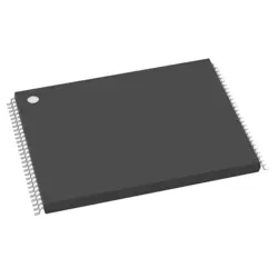

圖片僅供參考
SN54LS04J
IC INVERTER 6CH 6-INP 14CDIP
- 製造商
- 製造商。 部分 #SN54LS04J
- 包
- 資料表 SN54LS04J DataSheet
- 有現貨的6007
100%原創; 新
24小時準備發貨
365天保修
RFQ&; 獲得更多折扣
規格
| Series | 54LS |
| Part Status | Active |
| Logic Type | Inverter |
| Number of Circuits | 6 |
| Number of Inputs | 6 |
| Voltage - Supply | 4.5V ~ 5.5V |
| Current - Quiescent (Max) | 6.6 mA |
| Current - Output High, Low | 400µA, 4mA |
| Input Logic Level - Low | 0.7V |
| Input Logic Level - High | 2V |
| Max Propagation Delay @ V, Max CL | 15ns @ 5V, 15pF |
| Operating Temperature | -55°C ~ 125°C |
| Mounting Type | Through Hole |
| Supplier Device Package | 14-CDIP |
| Package / Case | 14-CDIP (0.300", 7.62mm) |
概述
Description
The SN54LS04J is a hex inverter integrated circuit (IC) belonging to the 74LS series of logic devices, designed for high-speed digital applications. It contains six independent inverter gates, each capable of converting a high logic level (1) to a low logic level (0) and vice versa. The device operates with a supply voltage typically ranging from 4.75V to 5.25V and is designed for TTL (Transistor-Transistor Logic) compatibility.
Key features include low power consumption, high noise immunity, and fast switching speeds, making it suitable for various applications in digital circuits, including signal conditioning, level shifting, and logic inversion. The SN54 series is classified as military-grade, ensuring reliability in harsh environments, while the LS designation indicates low power consumption compared to standard TTL ICs.
This IC is commonly used in digital systems for tasks requiring signal inversion and is available in dual-in-line (DIP) packages, facilitating easy integration into electronic projects and systems.
Features
The SN54LS04J is a hex inverter integrated circuit that belongs to the Low Power Schottky logic family. Key features include:
1. Six Inverters: Contains six independent inverter gates, allowing for versatile circuit designs.
2. Low Power Consumption: Operates with reduced power consumption compared to standard TTL devices, which makes it suitable for battery-operated applications.
3. High Speed: Offers fast switching times, typically around 10 ns, enabling high-speed operation in digital circuits.
4. Wide Supply Voltage: Compatible with a supply voltage range of 4.75V to 5.25V, making it flexible for various applications.
5. Temperature Range: Designed to function within a military temperature range of -55°C to +125°C, enhancing reliability in extreme environments.
6. Standard Pin Configuration: Features a standard 14-pin dual in-line package (DIP) for easy integration into various PCB designs.
7. Noise Margin: Provides excellent noise margins, improving signal integrity in digital circuits.
These features make the SN54LS04J suitable for various applications in digital logic and signal processing.
Package
The SN54LS04J is a hex inverter IC packaged in a dual in-line package (DIP) format, specifically a 14-pin plastic DIP.
Pinout
The SN54LS04J is a hex inverter IC that belongs to the 74LS series of logic devices. It has a pin count of 14. The function of the SN54LS04J is to perform logical inversion on input signals; it takes an input signal and produces the opposite output (i.e., if the input is high, the output is low, and vice versa) for each of its six inverter gates. The pin configuration includes:
- Pins 1, 2, 3, 4, 5, 6: Inputs for six inverter gates (A1 to A6).
- Pins 7, 9, 11, 13, 12, 10: Outputs corresponding to each inverter (Y1 to Y6).
- Pin 14: Vcc (positive power supply).
- Pin 7: Ground (GND).
The device operates with a typical supply voltage of 4.75V to 5.25V and is used in various digital logic applications for signal conditioning and logic level inversion.
Manufacturer
The SN54LS04J is manufactured by Texas Instruments (TI). Texas Instruments is a global technology company that designs and manufactures semiconductors and various integrated circuits. Founded in 1930, TI is known for its innovation in analog, embedded processing, and digital signal processing technologies. The company supplies products for a wide range of applications, including consumer electronics, automotive systems, industrial machinery, and communications. TI operates in multiple sectors, focusing on providing solutions that enhance performance and efficiency in electronic devices.
Application
The SN54LS04J is a hex inverter integrated circuit used in various applications, including digital logic circuits, signal conditioning, and waveform shaping. It's commonly utilized in computer systems, communication devices, and consumer electronics to perform logical operations, invert signals, and improve circuit reliability. Additionally, it can be employed in timing applications and as part of larger microcontroller or microprocessor designs.
Equivalent
The SN54LS04J is a hex inverter IC. Equivalent products include the SN74LS04N, 74HC04, 74HCT04, and 74LS04. These devices offer similar functionality, but ensure to check voltage levels and specifications for compatibility in your application.
船舶
運輸管道我們
通過DHL、FedEx、TNT、UPS或您選擇的任何其他貨運代理提供全球運輸服務。
運費參攷(DHL/FedEx):
動態主要裝載: 運費從25美元到45美元(0.5公斤)不等,預計交貨時間為2-5個工作日。
聯邦快遞: 運費從25美元到40美元(0.5公斤)不等,預計交貨時間為3-7個工作日。
不斷電供應系統: 運費從25美元到45美元(0.5公斤)不等,預計交貨時間為3-7個工作日。
三硝基甲苯: 運費從25美元到65美元(0.5公斤)不等,預計交貨時間為3-7個工作日。
增强型短消息: 運費從30美元到50美元(0.5公斤)不等,預計交貨時間為7-15個工作日。
掛號: 運費為2-4美元(0.1公斤),預計交貨時間為5-20個工作日。
支付
Payment Methods
付款條件為100%預付。
現時,我們只接受以下付款方式:
1. 貝寶
2. 信用卡/借記卡
3. 電匯
類似的
-
![MX25R8035FM1IL0]() MX25R8035FM1IL0
Macronix
-
![MX25L3233FM1I-08Q]() MX25L3233FM1I-08Q
Macronix
-
![MX25V4035FZUI]() MX25V4035FZUI
Macronix
-
![MX25V16066M1I02]() MX25V16066M1I02
Macronix
-
![MX30LF2G28AD-TI]() MX30LF2G28AD-TI
Macronix
-
![MX25R6435FBDIL0]() MX25R6435FBDIL0
Macronix
-
![MX25L25673GMI-10G]() MX25L25673GMI-10G
Macronix
-
![MX25V1635FM2I]() MX25V1635FM2I
Macronix
-
![MX25U3232FZBI02]() MX25U3232FZBI02
Macronix
-
![MX25L12835FZ2I-10G]() MX25L12835FZ2I-10..
Macronix
-
![MX25L25645GXDI-08G]() MX25L25645GXDI-08..
Macronix
-
![MX29F800CBTI-70G]() MX29F800CBTI-70G
Macronix