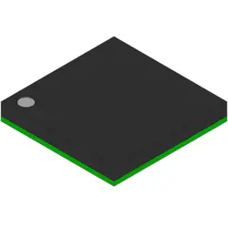
圖片僅供參考
SI5332BD11025-GM2
- 製造商
- 製造商。 部分 #SI5332BD11025-GM2
- 包 QFN-40
- 資料表 SI5332BD11025-GM2 DataSheet
- 有現貨的6139
100%原創; 新
24小時準備發貨
365天保修
RFQ&; 獲得更多折扣
規格
| Brand | Skyworks Solutions, Inc. |
| Packaging | Tray |
| Factory Pack Quantity:Factory Pack Quantity | 490 |
| Product Type | Clock Generators |
| Subcategory | Clock & Timer ICs |
| Mounting Style | SMD/SMT |
| Operating Supply Current | 45 mA |
| Minimum Operating Temperature | - 40 C |
| Maximum Operating Temperature | + 85 C |
| Type | Programmable Clock Generator |
| Number of Outputs | 8 Output |
| Max Output Freq | 200 MHz |
| Maximum Input Frequency | 250 MHz |
| Package/Case | QFN-40 |
| Duty Cycle - Max | 60 % |
| Supply Voltage - Max | 3.63 V |
| Supply Voltage - Min | 1.71 V |
| Operating Supply Voltage | 1.8 V, 2.5 V, 3.3 V |
| Output Type | HCSL, LVCMOS, LVDS, LVPECL |
| Jitter | 190 fs |
| Series | Si5332 |
| Development Kit | si5332-8ex-evb |
| Moisture Sensitive | Yes |
概述
Description
The SI5332BD11025-GM2 is a versatile clock generator and jitter cleaner from Silicon Labs, designed for high-performance applications. It features a programmable output frequency range from 2 kHz to 1 GHz, making it suitable for various applications such as telecommunications, networking, and data converters.
Key features include:
1. Multiple Outputs: It can provide up to 8 flexible output clocks with excellent phase noise performance.
2. Low Jitter: The device offers low phase jitter, which is crucial for maintaining signal integrity in high-speed digital systems.
3. Easy Configuration: The SI5332 can be configured via I²C, allowing users to set frequencies and output formats easily.
4. Power Efficiency: Designed for low power consumption, making it ideal for battery-operated devices.
5. Robust Performance: It supports various input reference sources and can operate across a wide range of supply voltages.
This component is widely used in applications that require precise timing, such as FPGA and ASIC designs, ensuring reliable performance in critical systems.
Key features include:
1. Multiple Outputs: It can provide up to 8 flexible output clocks with excellent phase noise performance.
2. Low Jitter: The device offers low phase jitter, which is crucial for maintaining signal integrity in high-speed digital systems.
3. Easy Configuration: The SI5332 can be configured via I²C, allowing users to set frequencies and output formats easily.
4. Power Efficiency: Designed for low power consumption, making it ideal for battery-operated devices.
5. Robust Performance: It supports various input reference sources and can operate across a wide range of supply voltages.
This component is widely used in applications that require precise timing, such as FPGA and ASIC designs, ensuring reliable performance in critical systems.
Features
The SI5332BD11025-GM2 is a versatile clock generator and jitter attenuator designed for various applications. Key features include:
1. High Performance: It offers low phase noise and low jitter outputs, making it suitable for high-speed data systems.
2. Output Frequencies: Supports multiple output frequencies ranging from 1 kHz to 1.1 GHz.
3. Clock Generation: Capable of generating multiple clock outputs with different frequencies from a single reference clock.
4. Programmability: Features I²C interface for flexible configuration and customization of output settings.
5. Multiple Output Formats: Supports various output formats including CMOS and LVDS.
6. Low Power Consumption: Designed for energy efficiency, making it ideal for battery-operated devices.
7. Temperature Range: Operates over a wide temperature range, enhancing reliability in various environments.
8. Small Package Size: Housed in a compact package, which is beneficial for space-constrained applications.
These features make the SI5332BD11025-GM2 suitable for applications in telecommunications, data centers, and consumer electronics.
1. High Performance: It offers low phase noise and low jitter outputs, making it suitable for high-speed data systems.
2. Output Frequencies: Supports multiple output frequencies ranging from 1 kHz to 1.1 GHz.
3. Clock Generation: Capable of generating multiple clock outputs with different frequencies from a single reference clock.
4. Programmability: Features I²C interface for flexible configuration and customization of output settings.
5. Multiple Output Formats: Supports various output formats including CMOS and LVDS.
6. Low Power Consumption: Designed for energy efficiency, making it ideal for battery-operated devices.
7. Temperature Range: Operates over a wide temperature range, enhancing reliability in various environments.
8. Small Package Size: Housed in a compact package, which is beneficial for space-constrained applications.
These features make the SI5332BD11025-GM2 suitable for applications in telecommunications, data centers, and consumer electronics.
Package
The SI5332BD11025-GM2 is packaged in a QFN (Quad Flat No-lead) form factor, specifically a 32-pin QFN package. This type of package provides a compact and efficient solution for surface mounting, offering good thermal performance and electrical characteristics.
Pinout
The SI5332BD11025-GM2 is a clock generator from Silicon Labs. It features a 32-pin QFN package.
Key pin functions include:
- Power Supply Pins: VDD and VDDIO for power.
- Ground Pins: GND for grounding.
- Input Pins: REF_CLK for external clock input.
- Output Pins: Multiple CLK outputs (such as CLKOUT0 to CLKOUT3) for distributing generated clocks.
- Control Pins: I2C interface pins (SDA and SCL) for configuration and control, along with a RESET pin for device reset.
- Status Pins: Various status outputs to indicate device status.
The device is primarily used for generating high-frequency clock signals for various applications, including networking and communication systems. The flexibility in output frequency and configurations makes it suitable for a wide range of digital systems.
Key pin functions include:
- Power Supply Pins: VDD and VDDIO for power.
- Ground Pins: GND for grounding.
- Input Pins: REF_CLK for external clock input.
- Output Pins: Multiple CLK outputs (such as CLKOUT0 to CLKOUT3) for distributing generated clocks.
- Control Pins: I2C interface pins (SDA and SCL) for configuration and control, along with a RESET pin for device reset.
- Status Pins: Various status outputs to indicate device status.
The device is primarily used for generating high-frequency clock signals for various applications, including networking and communication systems. The flexibility in output frequency and configurations makes it suitable for a wide range of digital systems.
Manufacturer
The manufacturer of the SI5332BD11025-GM2 is Silicon Labs, a technology company specializing in semiconductor solutions. Founded in 1996, Silicon Labs designs and develops a range of products, including microcontrollers, sensors, and wireless solutions, with a focus on connectivity and energy-efficient technologies. The SI5332 is a versatile clock generator known for its high performance and low power consumption, commonly used in applications such as communication systems, consumer electronics, and industrial automation. Silicon Labs is recognized for its innovation in the semiconductor industry and is committed to providing advanced solutions for a variety of markets.
Application
The SI5332BD11025-GM2 is a versatile clock generator and jitter attenuator used in applications such as telecommunications, data communications, networking equipment, audio/video processing, and industrial automation. It provides precise clock frequency generation and synchronization for systems requiring low jitter and high stability, making it suitable for 5G infrastructure, routers, servers, and digital signal processing applications.
Equivalent
The SI5332BD11025-GM2 is a clock generator and jitter attenuator. Equivalent products include the Texas Instruments CDCE6214, Analog Devices AD9576, and NXP/Freescale 74LVC1G, which offer similar functionalities in clock generation and synchronization. Always verify specific requirements and specifications, as performance and features may vary.
船舶
運輸管道我們
通過DHL、FedEx、TNT、UPS或您選擇的任何其他貨運代理提供全球運輸服務。
運費參攷(DHL/FedEx):
動態主要裝載: 運費從25美元到45美元(0.5公斤)不等,預計交貨時間為2-5個工作日。
聯邦快遞: 運費從25美元到40美元(0.5公斤)不等,預計交貨時間為3-7個工作日。
不斷電供應系統: 運費從25美元到45美元(0.5公斤)不等,預計交貨時間為3-7個工作日。
三硝基甲苯: 運費從25美元到65美元(0.5公斤)不等,預計交貨時間為3-7個工作日。
增强型短消息: 運費從30美元到50美元(0.5公斤)不等,預計交貨時間為7-15個工作日。
掛號: 運費為2-4美元(0.1公斤),預計交貨時間為5-20個工作日。
支付
Payment Methods
付款條件為100%預付。
現時,我們只接受以下付款方式:
1. 貝寶
2. 信用卡/借記卡
3. 電匯
類似的
-
![MX25R8035FM1IL0]() MX25R8035FM1IL0
MX25R8035FM1IL0
Macronix
-
![MX25L3233FM1I-08Q]() MX25L3233FM1I-08Q
MX25L3233FM1I-08Q
Macronix
-
![MX25V1635FZNI]() MX25V1635FZNI
MX25V1635FZNI
Macronix
-
![MX25V1635FZNQ03]() MX25V1635FZNQ03
MX25V1635FZNQ03
Macronix
-
![MX25V16066M2I02]() MX25V16066M2I02
MX25V16066M2I02
Macronix
-
![MX29GL512FHXFI-11G]() MX29GL512FHXFI-11..
MX29GL512FHXFI-11..
Macronix
-
![MX25U51279GXDR00]() MX25U51279GXDR00
MX25U51279GXDR00
Macronix
-
![MX25R1635FZUIH0]() MX25R1635FZUIH0
MX25R1635FZUIH0
Macronix
-
![MX25L6433FM2I-08G]() MX25L6433FM2I-08G
MX25L6433FM2I-08G
Macronix
-
![MX25L12833FZNI-10G]() MX25L12833FZNI-10..
MX25L12833FZNI-10..
Macronix
-
![MX66U1G45GMI00]() MX66U1G45GMI00
MX66U1G45GMI00
Macronix
-
![MX25R4035FM1IL0]() MX25R4035FM1IL0
MX25R4035FM1IL0
Macronix