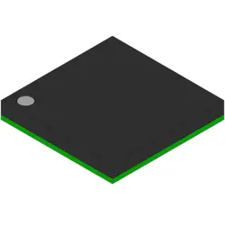
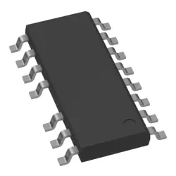
圖片僅供參考
S40FC004C1B1I00000
eMMC 4GB e.MMC5.1 BGA 13 x 11.5 x 0.8 mm STDF/W with tray packing
- 製造商
- 製造商。 部分 #S40FC004C1B1I00000
- 包
- 資料表 S40FC004C1B1I00000 DataSheet
- 有現貨的16203
100%原創; 新
24小時準備發貨
365天保修
RFQ&; 獲得更多折扣
規格
| Packaging | Tray |
| Standard Pack Qty | 171 |
概述
Description
S40FC004C1B1I00000 is a code that likely refers to a specific product or item, possibly in a catalog or inventory system. The format suggests it could denote a type of model, part number, or serial identifier typical in manufacturing, electronics, or software. Understanding the precise context of this code would require more information about the industry or field it pertains to. If you are looking for details about a specific product, technical specifications, or usage instructions, please provide additional context or clarify the domain in which this code is used.
Features
The S40FC004C1B1I00000 is a type of flash memory chip, specifically designed for embedded applications. Key features include:
1. Capacity: It typically offers a storage capacity of 4 Mbit.
2. Interface: Utilizes a Serial Peripheral Interface (SPI) for fast data transfer.
3. Voltage Range: Operates usually within a voltage range of 2.7V to 3.6V, making it suitable for various low-power applications.
4. Access Speed: Provides high-speed read/write operations, enhancing performance in data-intensive applications.
5. Data Retention: Offers a long data retention period, usually up to 20 years, ideal for critical data storage.
6. Endurance: Supports a significant number of program/erase cycles, typically around 100,000 cycles.
7. Form Factor: Available in compact packages suitable for space-constrained designs.
This chip is often used in consumer electronics, automotive, and industrial applications, where reliability and efficiency are paramount.
1. Capacity: It typically offers a storage capacity of 4 Mbit.
2. Interface: Utilizes a Serial Peripheral Interface (SPI) for fast data transfer.
3. Voltage Range: Operates usually within a voltage range of 2.7V to 3.6V, making it suitable for various low-power applications.
4. Access Speed: Provides high-speed read/write operations, enhancing performance in data-intensive applications.
5. Data Retention: Offers a long data retention period, usually up to 20 years, ideal for critical data storage.
6. Endurance: Supports a significant number of program/erase cycles, typically around 100,000 cycles.
7. Form Factor: Available in compact packages suitable for space-constrained designs.
This chip is often used in consumer electronics, automotive, and industrial applications, where reliability and efficiency are paramount.
Package
The S40FC004C1B1I00000 is typically packaged in a TSOP (Thin Small Outline Package) format. This type of package is designed for surface mounting, offering a compact footprint suitable for various electronic applications.
Pinout
The S40FC004C1B1I00000 is a 4 Mbit (512K x 8) Flash memory chip from Cypress Semiconductor (now part of Infineon Technologies). It typically features a 32-pin package and operates on a 3.0V to 3.6V power supply.
The main functions of the pins include:
1. Data Pins (DQ0-DQ7): These are the 8 data lines used for reading and writing data.
2. Address Pins (A0-A18): These pins are used to select the memory addresses.
3. Chip Enable (CE): Activates the chip for read/write operations.
4. Write Enable (WE): Controls write operations to the memory.
5. Output Enable (OE): Enables output data during read operations.
6. Reset (RESET): Resets the device to its initial state.
7. Vcc: Power supply pin.
8. GND: Ground pin.
It is used in various applications requiring non-volatile memory storage, such as firmware storage in embedded systems. Always refer to the specific datasheet for detailed information on pin configurations and electrical characteristics.
The main functions of the pins include:
1. Data Pins (DQ0-DQ7): These are the 8 data lines used for reading and writing data.
2. Address Pins (A0-A18): These pins are used to select the memory addresses.
3. Chip Enable (CE): Activates the chip for read/write operations.
4. Write Enable (WE): Controls write operations to the memory.
5. Output Enable (OE): Enables output data during read operations.
6. Reset (RESET): Resets the device to its initial state.
7. Vcc: Power supply pin.
8. GND: Ground pin.
It is used in various applications requiring non-volatile memory storage, such as firmware storage in embedded systems. Always refer to the specific datasheet for detailed information on pin configurations and electrical characteristics.
Manufacturer
The S40FC004C1B1I00000 is manufactured by Cypress Semiconductor Corporation. Cypress is a semiconductor company that specializes in designing and manufacturing a wide range of microcontrollers, memory products, and programmable components. Founded in 1982 and headquartered in San Jose, California, Cypress is known for its innovative solutions in the areas of embedded systems, connectivity, and memory technologies. The company serves various markets, including automotive, industrial, consumer electronics, and IoT. In 2020, Cypress was acquired by Infineon Technologies, a major player in the semiconductor industry, further expanding its capabilities and market reach.
Application
S40FC004C1B1I00000 is a type of flash memory chip typically used in various application areas, including embedded systems, IoT devices, consumer electronics, automotive applications, and industrial automation. Its features make it suitable for data storage in firmware, configuration settings, and applications requiring reliable non-volatile memory solutions.
Equivalent
The S40FC004C1B1I00000 chip is a NAND Flash memory device. Equivalent products may include similar NAND Flash chips from manufacturers like Micron (MT29F4G08ABAEAWP), Samsung (K9F4G08U0M), and Intel (29F4G08ABABA). Specific equivalents depend on requirements like density, package type, and performance specifications. Always confirm compatibility with datasheets before substituting components.
船舶
運輸管道我們
通過DHL、FedEx、TNT、UPS或您選擇的任何其他貨運代理提供全球運輸服務。
運費參攷(DHL/FedEx):
動態主要裝載: 運費從25美元到45美元(0.5公斤)不等,預計交貨時間為2-5個工作日。
聯邦快遞: 運費從25美元到40美元(0.5公斤)不等,預計交貨時間為3-7個工作日。
不斷電供應系統: 運費從25美元到45美元(0.5公斤)不等,預計交貨時間為3-7個工作日。
三硝基甲苯: 運費從25美元到65美元(0.5公斤)不等,預計交貨時間為3-7個工作日。
增强型短消息: 運費從30美元到50美元(0.5公斤)不等,預計交貨時間為7-15個工作日。
掛號: 運費為2-4美元(0.1公斤),預計交貨時間為5-20個工作日。
支付
Payment Methods
付款條件為100%預付。
現時,我們只接受以下付款方式:
1. 貝寶
2. 信用卡/借記卡
3. 電匯
類似的
-
![MX25V16066M2I02]() MX25V16066M2I02
MX25V16066M2I02
Macronix
-
![MX29GL512FHXFI-11G]() MX29GL512FHXFI-11..
MX29GL512FHXFI-11..
Macronix
-
![MX25U51279GXDR00]() MX25U51279GXDR00
MX25U51279GXDR00
Macronix
-
![MX25U25643GZNI00]() MX25U25643GZNI00
MX25U25643GZNI00
Macronix
-
![MX25U3232FZBI02]() MX25U3232FZBI02
MX25U3232FZBI02
Macronix
-
![MX25L6433FM2I-08G]() MX25L6433FM2I-08G
MX25L6433FM2I-08G
Macronix
-
![MX25U25645GXDI00]() MX25U25645GXDI00
MX25U25645GXDI00
Macronix
-
![MX29LV160DTTI-70G]() MX29LV160DTTI-70G
MX29LV160DTTI-70G
Macronix
-
![MX25L25645GXDI-08G]() MX25L25645GXDI-08..
MX25L25645GXDI-08..
Macronix
-
![MX29F040CTI-70G]() MX29F040CTI-70G
MX29F040CTI-70G
Macronix
-
![MX29LV640ETTI-70G]() MX29LV640ETTI-70G
MX29LV640ETTI-70G
Macronix
-
![MX25L25735FMI-10G]() MX25L25735FMI-10G
MX25L25735FMI-10G
Macronix