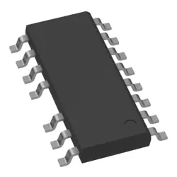
圖片僅供參考
S40FC002C1B2I00000
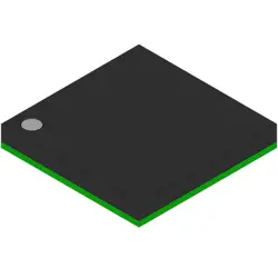
eMMC 2GB e.MMC5.1 BGA 9.0 x 7.5 x 0.8 mm Industrial Grade with tray packing
- 製造商
- 製造商。 部分 #S40FC002C1B2I00000
- 包
- 資料表 S40FC002C1B2I00000 DataSheet
- 有現貨的11439
100%原創; 新
24小時準備發貨
365天保修
RFQ&; 獲得更多折扣
規格
| Packaging | Tray |
| Standard Pack Qty | 225 |
概述
Description
The term "S40FC002C1B2I00000" appears to refer to a specific code or identifier, likely related to a product, device, or system. However, without additional context, it's challenging to provide a precise introduction or explanation. In general, such alphanumeric codes could denote various attributes, including model numbers, serial numbers, or configuration IDs for electronics, machinery, or software applications.
If this code pertains to a particular industry, product line, or technology, please provide more details for a more tailored response. Understanding the background, such as whether it relates to computing, telecommunications, automotive, or another field, would greatly help clarify its significance and applications.
If this code pertains to a particular industry, product line, or technology, please provide more details for a more tailored response. Understanding the background, such as whether it relates to computing, telecommunications, automotive, or another field, would greatly help clarify its significance and applications.
Features
The S40FC002C1B2I00000 is a specific model of a storage component, likely a NAND flash memory or similar device. While detailed specifications for this exact model may not be widely available, typical features of such components include:
1. Capacity: Usually offers substantial storage capacity, suitable for various applications.
2. Interface: Often utilizes high-speed interfaces like SPI or NAND interface for fast data transfer.
3. Durability: Designed for reliability with wear leveling and error correction mechanisms to extend lifespan.
4. Form Factor: Compact design suitable for integration into various electronic devices.
5. Power Efficiency: Optimized for low power consumption, enhancing battery life in portable devices.
6. Temperature Range: Operates in a broad temperature range, ensuring functionality in diverse environments.
For precise specifications, it is recommended to consult the manufacturer's datasheet or technical documentation.
1. Capacity: Usually offers substantial storage capacity, suitable for various applications.
2. Interface: Often utilizes high-speed interfaces like SPI or NAND interface for fast data transfer.
3. Durability: Designed for reliability with wear leveling and error correction mechanisms to extend lifespan.
4. Form Factor: Compact design suitable for integration into various electronic devices.
5. Power Efficiency: Optimized for low power consumption, enhancing battery life in portable devices.
6. Temperature Range: Operates in a broad temperature range, ensuring functionality in diverse environments.
For precise specifications, it is recommended to consult the manufacturer's datasheet or technical documentation.
Package
The S40FC002C1B2I00000 is typically packaged in a TSOP (Thin Small Outline Package) format, which is designed for compactness and efficiency in electronic devices.
Pinout
The S40FC002C1B2I00000 is a 2 Megabit (256 K x 8) Flash memory device manufactured by Spansion (now part of Cypress Semiconductor). It features a total of 32 pins.
The primary functions of these pins include:
- Address pins (A0-A17): Used to select the memory location for read or write operations.
- Data pins (DQ0-DQ7): Bidirectional data bus for data input and output during read/write operations.
- Chip Enable (CE): Activates the chip for operation.
- Output Enable (OE): Controls the output of data.
- Write Enable (WE): Allows data to be written to the memory.
- Reset (RESET): Resets the device for initialization.
- Program/Erase (WP): Write protect feature to prevent accidental writes.
- Vcc and Vss: Power supply and ground connections.
This configuration supports asynchronous read and write operations, making it suitable for various embedded applications.
The primary functions of these pins include:
- Address pins (A0-A17): Used to select the memory location for read or write operations.
- Data pins (DQ0-DQ7): Bidirectional data bus for data input and output during read/write operations.
- Chip Enable (CE): Activates the chip for operation.
- Output Enable (OE): Controls the output of data.
- Write Enable (WE): Allows data to be written to the memory.
- Reset (RESET): Resets the device for initialization.
- Program/Erase (WP): Write protect feature to prevent accidental writes.
- Vcc and Vss: Power supply and ground connections.
This configuration supports asynchronous read and write operations, making it suitable for various embedded applications.
Manufacturer
The S40FC002C1B2I00000 is manufactured by NXP Semiconductors, a global semiconductor company. NXP specializes in a wide range of products, including microcontrollers, processors, and integrated circuits, primarily for automotive, industrial, and consumer electronics applications. The company focuses on providing solutions for secure connectivity and processing, catering to applications such as smart devices, automotive systems, and the Internet of Things (IoT). NXP was formed from the spinoff of Philips' semiconductor division and has established itself as a leader in the semiconductor industry, known for innovation and high-performance products.
Application
The S40FC002C1B2I00000 is a specialized semiconductor device used primarily in automotive, industrial, and consumer electronics applications. Its features make it suitable for power management, signal processing, and communication systems. It can be utilized in battery management systems, motor control, and various sensor interfaces, contributing to improved efficiency and performance in electronic designs.
Equivalent
The S40FC002C1B2I00000 chip is a NOR Flash memory device. Equivalent products may include:
1. S29GL032N - Similar density and technology.
2. M25P32 - Comparable performance and specification.
3. AT45DB321E - Flash memory with similar features.
4. W25Q32JV - A competitor with similar capacity and interface.
Always verify specific pin configurations and electrical characteristics for compatibility.
1. S29GL032N - Similar density and technology.
2. M25P32 - Comparable performance and specification.
3. AT45DB321E - Flash memory with similar features.
4. W25Q32JV - A competitor with similar capacity and interface.
Always verify specific pin configurations and electrical characteristics for compatibility.
船舶
運輸管道我們
通過DHL、FedEx、TNT、UPS或您選擇的任何其他貨運代理提供全球運輸服務。
運費參攷(DHL/FedEx):
動態主要裝載: 運費從25美元到45美元(0.5公斤)不等,預計交貨時間為2-5個工作日。
聯邦快遞: 運費從25美元到40美元(0.5公斤)不等,預計交貨時間為3-7個工作日。
不斷電供應系統: 運費從25美元到45美元(0.5公斤)不等,預計交貨時間為3-7個工作日。
三硝基甲苯: 運費從25美元到65美元(0.5公斤)不等,預計交貨時間為3-7個工作日。
增强型短消息: 運費從30美元到50美元(0.5公斤)不等,預計交貨時間為7-15個工作日。
掛號: 運費為2-4美元(0.1公斤),預計交貨時間為5-20個工作日。
支付
Payment Methods
付款條件為100%預付。
現時,我們只接受以下付款方式:
1. 貝寶
2. 信用卡/借記卡
3. 電匯
類似的
-
![MX66U1G45GXDI00]() MX66U1G45GXDI00
MX66U1G45GXDI00
Macronix
-
![MX25V5126FM1I]() MX25V5126FM1I
MX25V5126FM1I
Macronix
-
![MX25R3235FZNIL0]() MX25R3235FZNIL0
MX25R3235FZNIL0
Macronix
-
![MX29GL512FHXFI-11G]() MX29GL512FHXFI-11..
MX29GL512FHXFI-11..
Macronix
-
![MX25U51279GXDR00]() MX25U51279GXDR00
MX25U51279GXDR00
Macronix
-
![MX25U3232FZBI02]() MX25U3232FZBI02
MX25U3232FZBI02
Macronix
-
![MX25L6433FM2I-08G]() MX25L6433FM2I-08G
MX25L6433FM2I-08G
Macronix
-
![MX25U6435FM2I-10G]() MX25U6435FM2I-10G
MX25U6435FM2I-10G
Macronix
-
![MX25L12833FZNI-10G]() MX25L12833FZNI-10..
MX25L12833FZNI-10..
Macronix
-
![MX25L25645GXDI-08G]() MX25L25645GXDI-08..
MX25L25645GXDI-08..
Macronix
-
![MX29F040CTI-70G]() MX29F040CTI-70G
MX29F040CTI-70G
Macronix
-
![MX25L25735FMI-10G]() MX25L25735FMI-10G
MX25L25735FMI-10G
Macronix