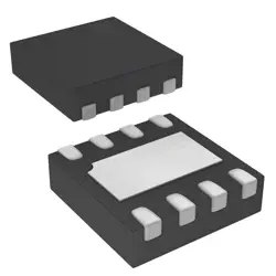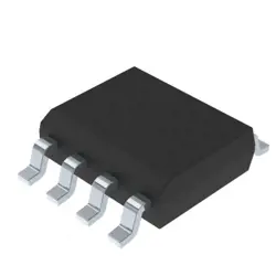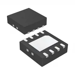
圖片僅供參考
PCF8591T/2
Real Time Clock PCF8591T/SO16//2/REEL 13 Q1/T1 *STANDARD MARK SMD
- 製造商
- 製造商。 部分 #PCF8591T/2
- 包
- 資料表
- 有現貨的18488
100%原創; 新
24小時準備發貨
365天保修
RFQ&; 獲得更多折扣
規格
概述
Description
The PCF8591T/2 is an integrated circuit designed for data acquisition and signal processing, featuring a 4-channel analog-to-digital converter (ADC) and a digital-to-analog converter (DAC). It operates over an I2C interface, allowing for easy communication with microcontrollers and other digital systems.
The device includes:
1. 4 ADC Channels: It can convert four separate analog signals to digital form with a 10-bit resolution, making it suitable for various sensor applications.
2. 1 DAC Channel: It provides a single output channel, enabling the generation of analog signals from digital values.
3. I2C Interface: The PCF8591T/2 supports multiple devices on a single bus, allowing for extensive flexibility in circuit design.
4. Low Power Consumption: It operates effectively in low-power environments, making it suitable for battery-operated devices.
Applications include industrial automation, environmental monitoring, and any system requiring analog signal processing. Its compact design and versatility make it a popular choice in embedded systems.
Features
The PCF8591T/2 is an integrated circuit designed for analog-to-digital and digital-to-analog conversion. Key features include:
1. Analog Inputs: It has four single-ended input channels (A0 to A3), allowing for the measurement of analog signals.
2. Digital Outputs: One 8-bit digital-to-analog converter (DAC) output, which can generate variable analog voltages.
3. I2C Interface: Communication via I2C, supporting multiple devices on the same bus with a 7-bit address.
4. Resolution: Provides 8-bit resolution for both ADC and DAC, allowing for 256 distinct levels.
5. Sample Rate: Capable of sampling rates up to 100 kHz, suitable for most basic applications.
6. Power Supply: Operates on a supply voltage range of 2.5V to 6V, making it compatible with various microcontrollers.
7. Low Power Consumption: Designed for low power usage, ideal for battery-operated devices.
8. Internal Reference: Includes an internal reference voltage for consistent performance across varying conditions.
These features make the PCF8591T/2 a versatile choice for applications involving data acquisition and signal processing.
Package
The PCF8591T/2 is typically available in a DIP-8 (Dual In-line Package with 8 pins) format. This package type facilitates easy integration onto printed circuit boards (PCBs) for various electronic applications, particularly in analog-to-digital conversion tasks.
Pinout
The PCF8591T/2 is an I2C bus-compatible 8-bit ADC (Analog-to-Digital Converter) and DAC (Digital-to-Analog Converter) IC. It features a total of 8 pins:
1. VDD: Supply voltage (typically +2.7V to +6V).
2. VSS: Ground connection.
3. SDA: Serial Data Line for I2C communication.
4. SCL: Serial Clock Line for I2C communication.
5. A0: Address pin used to set the I2C address (can be connected to GND or VDD).
6. A1: Address pin for further address configuration.
7. A2: Address pin for additional address setting.
8. OUT: Analog output for the DAC (used for voltage output).
The IC supports up to four analog input channels (labeled as AIN0 to AIN3) for the ADC functionality and includes one DAC output. It is widely used in sensor applications and data acquisition systems.
Manufacturer
The PCF8591T/2 is manufactured by NXP Semiconductors, a global semiconductor company headquartered in Eindhoven, Netherlands. NXP specializes in designing and manufacturing integrated circuits, specifically for automotive, industrial, and Internet of Things (IoT) applications. The company is known for its innovation in areas such as secure connectivity, processing, and sensing solutions, focusing on providing high-performance semiconductor products to enhance electronic systems across various industries. NXP was formed in 2006 after the spin-off of Philips' semiconductor division and has since established itself as a leader in the semiconductor market, particularly in developing solutions for embedded systems and wireless communication.
Application
The PCF8591T/2 is an I2C-compatible analog-to-digital converter (ADC) and digital-to-analog converter (DAC) used in various applications, including:
1. Sensor Interfacing: Reading analog sensors like temperature, light, and pressure sensors.
2. Data Acquisition: Collecting and processing analog signals for monitoring systems.
3. Embedded Systems: Used in microcontroller projects for signal processing.
4. Audio Applications: Converting digital audio signals to analog for playback.
5. Control Systems: Generating control signals in automation and robotics.
Equivalent
Equivalent products to the PCF8591T/2 chip include the MCP3004/3008 from Microchip, the ADS1115 from Texas Instruments, and the MAX11614 from Maxim Integrated. These alternatives offer similar functionalities for analog-to-digital conversion and are suitable for various applications in embedded systems. Always check specifications for compatibility with your specific requirements.
船舶
運輸管道我們
通過DHL、FedEx、TNT、UPS或您選擇的任何其他貨運代理提供全球運輸服務。
運費參攷(DHL/FedEx):
動態主要裝載: 運費從25美元到45美元(0.5公斤)不等,預計交貨時間為2-5個工作日。
聯邦快遞: 運費從25美元到40美元(0.5公斤)不等,預計交貨時間為3-7個工作日。
不斷電供應系統: 運費從25美元到45美元(0.5公斤)不等,預計交貨時間為3-7個工作日。
三硝基甲苯: 運費從25美元到65美元(0.5公斤)不等,預計交貨時間為3-7個工作日。
增强型短消息: 運費從30美元到50美元(0.5公斤)不等,預計交貨時間為7-15個工作日。
掛號: 運費為2-4美元(0.1公斤),預計交貨時間為5-20個工作日。
支付
Payment Methods
付款條件為100%預付。
現時,我們只接受以下付款方式:
1. 貝寶
2. 信用卡/借記卡
3. 電匯
類似的
-
![MX25L3233FZBI-08Q]() MX25L3233FZBI-08Q
Macronix
-
![MX25V5126FM1I]() MX25V5126FM1I
Macronix
-
![MX25V4035FZUI]() MX25V4035FZUI
Macronix
-
![MX25V2033FM1I]() MX25V2033FM1I
Macronix
-
![MX25V16066M2I02]() MX25V16066M2I02
Macronix
-
![MX25U25643GZNI00]() MX25U25643GZNI00
Macronix
-
![MX25L2006EM1I-12G]() MX25L2006EM1I-12G
Macronix
-
![MX25R1635FZUIH0]() MX25R1635FZUIH0
Macronix
-
![MX25V1635FM2I]() MX25V1635FM2I
Macronix
-
![MX25L6433FM2I-08G]() MX25L6433FM2I-08G
Macronix
-
![MX25U6435FM2I-10G]() MX25U6435FM2I-10G
Macronix
-
![MX25L12833FZNI-10G]() MX25L12833FZNI-10..
Macronix