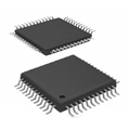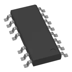

圖片僅供參考
PCA9617ADP
LEVEL TRANSLATING FM+ I2C-BUS
- 製造商
- 製造商。 部分 #PCA9617ADP
- 包 TSSOP-8
- 資料表 PCA9617ADP DataSheet
- 有現貨的5490
100%原創; 新
24小時準備發貨
365天保修
RFQ&; 獲得更多折扣
規格
| Package | Bulk |
| ProductStatus | Active |
概述
Description
The PCA9617ADP is a dual bidirectional I²C bus and SMBus level shifter designed to enable communication between devices operating at different voltage levels. This device helps interface 1.8V to 5V I²C buses, making it suitable for mixed-voltage systems.
Key features include:
- Dual-channel operation: Allows for bidirectional communication over two separate channels.
- Wide voltage range: Supports I²C devices operating at 1.8V, 2.5V, 3.3V, or 5V.
- Low power consumption: Ideal for battery-operated devices.
- Built-in pull-up resistors: Simplifies circuit design by integrating necessary components.
- Fast data rates: Supports standard (100 kHz) and fast-mode (400 kHz) I²C communication.
The PCA9617ADP is typically used in applications such as sensor interfaces, consumer electronics, and communication devices where level shifting is required. Its compact design and ease of use make it a popular choice for engineers working with multi-voltage systems.
Features
The PCA9617ADP is a high-speed I²C and SMBus bus buffer designed to extend the range and improve signal integrity of I²C communication. Key features include:
1. Dual-Channel Design: Supports two channels for bi-directional data transfer.
2. Bus Voltage Level Translation: Operates with VCC ranges from 1.8V to 5.5V, allowing interconnection between different voltage levels.
3. High-Speed Operation: Supports standard mode (up to 100 kHz), fast mode (up to 400 kHz), and fast-mode plus (up to 1 MHz).
4. Low Power Consumption: Consumes minimal power in standby mode, enhancing efficiency.
5. Open-Drain Output Configuration: Compatible with open-drain I²C devices.
6. Short-Circuit Protection: Provides robustness against accidental short circuits.
7. Thermal Shutdown: Integrated thermal protection to prevent overheating.
8. Wide Operating Temperature Range: Suitable for industrial applications.
These features make the PCA9617ADP ideal for applications requiring reliable I²C communication over longer distances or with mixed voltage systems.
Package
The PCA9617ADP is available in a TSSOP-16 (Thin Shrink Small Outline Package) package type.
Pinout
The PCA9617ADP is a dual I2C-bus and SMBus buffer with a total of 8 pins.
Pin Count and Functions:
1. VCC (Pin 1): Power supply.
2. GND (Pin 2): Ground.
3. SDA1 (Pin 3): I2C data line input/output for bus 1.
4. SCL1 (Pin 4): I2C clock line input/output for bus 1.
5. SDA2 (Pin 5): I2C data line input/output for bus 2.
6. SCL2 (Pin 6): I2C clock line input/output for bus 2.
7. A1 (Pin 7): Input for bus 1; determines the direction of the buffer.
8. A2 (Pin 8): Input for bus 2; determines the direction of the buffer.
The PCA9617ADP is designed to extend I2C/SMBus communications over longer distances and provides voltage level shifting between different I2C bus voltage levels.
Manufacturer
The PCA9617ADP is manufactured by NXP Semiconductors, a global semiconductor company known for its innovative products in automotive, industrial, and Internet of Things (IoT) applications. NXP focuses on providing high-performance mixed-signal and digital semiconductor solutions, including microcontrollers, processors, and connectivity solutions. The company, formed from the spin-off of Philips’ semiconductor division in 2006, has a strong emphasis on developing technologies that enable secure connections and smart experiences across various industries. NXP is recognized for its leadership in automotive electronics and has a significant presence in security and IoT markets.
Application
The PCA9617ADP is a dual I²C bus extender designed for various applications, including communication between I²C devices over longer distances, connecting multiple I²C buses, and interfacing with devices operating at different voltage levels. It is commonly used in industrial automation, consumer electronics, medical devices, and automotive systems, facilitating reliable data transfer in complex systems with multiple I²C peripherals.
Equivalent
The PCA9617ADP is a dual bidirectional I2C bus buffer. Equivalent products include:
1. PCA9515A
2. PCA9516A
3. TCA9517
4. TCA9406
These chips also serve as I2C bus buffers and level shifters, offering similar functionalities. Always verify specifications for compatibility with your specific application.
1. PCA9515A
2. PCA9516A
3. TCA9517
4. TCA9406
These chips also serve as I2C bus buffers and level shifters, offering similar functionalities. Always verify specifications for compatibility with your specific application.
船舶
運輸管道我們
通過DHL、FedEx、TNT、UPS或您選擇的任何其他貨運代理提供全球運輸服務。
運費參攷(DHL/FedEx):
動態主要裝載: 運費從25美元到45美元(0.5公斤)不等,預計交貨時間為2-5個工作日。
聯邦快遞: 運費從25美元到40美元(0.5公斤)不等,預計交貨時間為3-7個工作日。
不斷電供應系統: 運費從25美元到45美元(0.5公斤)不等,預計交貨時間為3-7個工作日。
三硝基甲苯: 運費從25美元到65美元(0.5公斤)不等,預計交貨時間為3-7個工作日。
增强型短消息: 運費從30美元到50美元(0.5公斤)不等,預計交貨時間為7-15個工作日。
掛號: 運費為2-4美元(0.1公斤),預計交貨時間為5-20個工作日。
支付
Payment Methods
付款條件為100%預付。
現時,我們只接受以下付款方式:
1. 貝寶
2. 信用卡/借記卡
3. 電匯
類似的
-
![MX25V1635FZNI]() MX25V1635FZNI
Macronix
-
![MX29F400CBTI-70G]() MX29F400CBTI-70G
Macronix
-
![MX25V2033FM1I]() MX25V2033FM1I
Macronix
-
![MX25V16066M1I02]() MX25V16066M1I02
Macronix
-
![MX25L8035EM2I-10G]() MX25L8035EM2I-10G
Macronix
-
![MX25U25643GZNI00]() MX25U25643GZNI00
Macronix
-
![MX25U6435FM2I-10G]() MX25U6435FM2I-10G
Macronix
-
![MX25U25645GXDI00]() MX25U25645GXDI00
Macronix
-
![MX29LV160DTTI-70G]() MX29LV160DTTI-70G
Macronix
-
![MX25L25645GXDI-08G]() MX25L25645GXDI-08..
Macronix
-
![MX29F800CBTI-70G]() MX29F800CBTI-70G
Macronix
-
![MX25L25735FMI-10G]() MX25L25735FMI-10G
Macronix