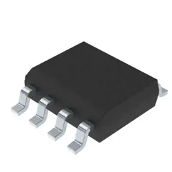
圖片僅供參考
NCV887302D1R2G
AUTOMOTIVE SWITCHER
- 製造商
- 製造商。 部分 #NCV887302D1R2G
- 包 SOIC-8
- 資料表
- 有現貨的7638
100%原創; 新
24小時準備發貨
365天保修
RFQ&; 獲得更多折扣
規格
| Package | Tape & Reel (TR),Cut Tape (CT) |
| ProductStatus | Active |
| OutputType | Transistor Driver |
| Function | Step-Up |
| OutputConfiguration | Positive |
| Topology | Boost |
| NumberofOutputs | 1 |
| OutputPhases | 1 |
| Voltage-Supply(Vcc/Vdd) | 3.2V ~ 40V |
| Frequency-Switching | 400kHz |
| DutyCycle(Max) | 92.5% |
| SynchronousRectifier | No |
| ClockSync | Yes |
| ControlFeatures | Current Sense, Enable |
| OperatingTemperature | -40°C ~ 150°C (TJ) |
| MountingType | Surface Mount |
| Package/Case | 8-SOIC (0.154, 3.90mm Width) |
概述
Description
The NCV887302D1R2G is a controller designed for automotive applications, specifically for single-ended primary-inductor converter (SEPIC) configurations. Manufactured by ON Semiconductor, it is used to manage the power conversion process in automotive systems, such as LED lighting, battery charging, and other applications requiring a step-up or step-down voltage conversion.
Key features of the NCV887302D1R2G include its wide input voltage range, which makes it suitable for various automotive power systems. It also offers a robust set of protections, including undervoltage lockout (UVLO), overcurrent protection (OCP), and thermal shutdown, enhancing its reliability and safety in harsh automotive environments.
The device operates in a fixed frequency mode and supports pulse-width modulation (PWM) for maintaining efficient power conversion. Additionally, it includes a built-in gate driver for driving external MOSFETs, which aids in reducing component count and simplifying circuit design.
Overall, the NCV887302D1R2G is a versatile and reliable choice for engineers designing power management systems in automotive applications.
Key features of the NCV887302D1R2G include its wide input voltage range, which makes it suitable for various automotive power systems. It also offers a robust set of protections, including undervoltage lockout (UVLO), overcurrent protection (OCP), and thermal shutdown, enhancing its reliability and safety in harsh automotive environments.
The device operates in a fixed frequency mode and supports pulse-width modulation (PWM) for maintaining efficient power conversion. Additionally, it includes a built-in gate driver for driving external MOSFETs, which aids in reducing component count and simplifying circuit design.
Overall, the NCV887302D1R2G is a versatile and reliable choice for engineers designing power management systems in automotive applications.
Features
The NCV887302D1R2G is a boost controller designed for automotive applications. It is a part of ON Semiconductor's product line and offers several key features:
1. Wide Operating Range: The controller supports a wide input voltage range, which is ideal for automotive environments where voltage can vary significantly.
2. External FET Control: It utilizes an external N-channel MOSFET for switching, providing flexibility in power handling and efficiency optimization.
3. Low Quiescent Current: The device is designed to consume minimal power when not in active operation, enhancing battery life.
4. Programmable Features: It offers programmable soft-start, overvoltage protection, and switching frequency, allowing customization for specific applications.
5. Protection Features: The controller includes features like over-current protection, thermal shutdown, and undervoltage lockout to ensure safe operation under various conditions.
6. Synchronization Capability: It can be synchronized to an external clock, which helps in reducing electromagnetic interference and improving performance.
7. Automotive Grade: It meets automotive standards, ensuring reliability and robustness for use in vehicles.
Overall, the NCV887302D1R2G is designed to efficiently manage power conversion in demanding automotive environments, offering flexibility and a range of protective features.
1. Wide Operating Range: The controller supports a wide input voltage range, which is ideal for automotive environments where voltage can vary significantly.
2. External FET Control: It utilizes an external N-channel MOSFET for switching, providing flexibility in power handling and efficiency optimization.
3. Low Quiescent Current: The device is designed to consume minimal power when not in active operation, enhancing battery life.
4. Programmable Features: It offers programmable soft-start, overvoltage protection, and switching frequency, allowing customization for specific applications.
5. Protection Features: The controller includes features like over-current protection, thermal shutdown, and undervoltage lockout to ensure safe operation under various conditions.
6. Synchronization Capability: It can be synchronized to an external clock, which helps in reducing electromagnetic interference and improving performance.
7. Automotive Grade: It meets automotive standards, ensuring reliability and robustness for use in vehicles.
Overall, the NCV887302D1R2G is designed to efficiently manage power conversion in demanding automotive environments, offering flexibility and a range of protective features.
Package
The NCV887302D1R2G is housed in a SOIC-8 package. This is a small outline integrated circuit with 8 pins, commonly used for surface-mount technology applications.
Pinout
The NCV887302D1R2G is a non-synchronous boost controller with a wide input voltage range, designed for automotive applications. It is built to operate in harsh environments and offers robust functionality.
This device typically comes in a SOIC-8 package, which has a total of 8 pins. The general pin functions for such a device are as follows:
1. VCC: Power supply input.
2. GND: Ground connection.
3. SW: Switch node; connects to the inductor and diode.
4. FB: Feedback pin; provides output voltage regulation by comparing the feedback voltage to an internal reference.
5. COMP: Compensation pin; used for stability and dynamic response control.
6. EN/SYNC: Enable or synchronization input; used to enable the device or synchronize its operation with an external clock.
7. ISNS: Current sense input; monitors the inductor current for over-current protection.
8. SS: Soft-start control; manages the ramp-up time of the output voltage to limit inrush current.
For precise pin functions and configuration, it is advisable to consult the specific datasheet or technical documentation provided by the manufacturer.
This device typically comes in a SOIC-8 package, which has a total of 8 pins. The general pin functions for such a device are as follows:
1. VCC: Power supply input.
2. GND: Ground connection.
3. SW: Switch node; connects to the inductor and diode.
4. FB: Feedback pin; provides output voltage regulation by comparing the feedback voltage to an internal reference.
5. COMP: Compensation pin; used for stability and dynamic response control.
6. EN/SYNC: Enable or synchronization input; used to enable the device or synchronize its operation with an external clock.
7. ISNS: Current sense input; monitors the inductor current for over-current protection.
8. SS: Soft-start control; manages the ramp-up time of the output voltage to limit inrush current.
For precise pin functions and configuration, it is advisable to consult the specific datasheet or technical documentation provided by the manufacturer.
Manufacturer
The NCV887302D1R2G is manufactured by ON Semiconductor, which is now known as onsemi. Onsemi is a leading semiconductor supplier that focuses on energy-efficient electronics. The company provides a wide range of products, including sensors, power management components, analog devices, and connectivity solutions. Their products are utilized in various sectors such as automotive, industrial, communications, computing, and consumer applications.
Application
The NCV887302D1R2G is a versatile automotive-grade boost controller IC used in various applications, including automotive power management systems, DC-DC boost converters, start-stop systems, and cold-crank voltage stabilization. It helps maintain stable voltage levels, ensuring reliable performance in vehicles despite fluctuating battery conditions.
Equivalent
Equivalent products to the NCV887302D1R2G chip, which is an automotive-grade, non-synchronous boost controller, include:
1. Texas Instruments LM3481: A versatile controller for boost and SEPIC applications.
2. Microchip MCP1650: A boost controller with wide input range.
3. Maxim Integrated MAX1771: A high-efficiency boost controller suitable for similar applications.
4. Analog Devices LT3757: Offers high voltage boost capabilities.
Ensure the chosen equivalent meets specific application requirements like voltage, current, and switching frequency.
1. Texas Instruments LM3481: A versatile controller for boost and SEPIC applications.
2. Microchip MCP1650: A boost controller with wide input range.
3. Maxim Integrated MAX1771: A high-efficiency boost controller suitable for similar applications.
4. Analog Devices LT3757: Offers high voltage boost capabilities.
Ensure the chosen equivalent meets specific application requirements like voltage, current, and switching frequency.
船舶
運輸管道我們
通過DHL、FedEx、TNT、UPS或您選擇的任何其他貨運代理提供全球運輸服務。
運費參攷(DHL/FedEx):
動態主要裝載: 運費從25美元到45美元(0.5公斤)不等,預計交貨時間為2-5個工作日。
聯邦快遞: 運費從25美元到40美元(0.5公斤)不等,預計交貨時間為3-7個工作日。
不斷電供應系統: 運費從25美元到45美元(0.5公斤)不等,預計交貨時間為3-7個工作日。
三硝基甲苯: 運費從25美元到65美元(0.5公斤)不等,預計交貨時間為3-7個工作日。
增强型短消息: 運費從30美元到50美元(0.5公斤)不等,預計交貨時間為7-15個工作日。
掛號: 運費為2-4美元(0.1公斤),預計交貨時間為5-20個工作日。
支付
Payment Methods
付款條件為100%預付。
現時,我們只接受以下付款方式:
1. 貝寶
2. 信用卡/借記卡
3. 電匯
類似的
-
![MX25V1635FZNI]() MX25V1635FZNI
MX25V1635FZNI
Macronix
-
![MX25R3235FZNIL0]() MX25R3235FZNIL0
MX25R3235FZNIL0
Macronix
-
![MX30LF2G28AD-TI]() MX30LF2G28AD-TI
MX30LF2G28AD-TI
Macronix
-
![MX25L8035EM2I-10G]() MX25L8035EM2I-10G
MX25L8035EM2I-10G
Macronix
-
![MX29GL512FHXFI-11G]() MX29GL512FHXFI-11..
MX29GL512FHXFI-11..
Macronix
-
![MX25V1635FM2I]() MX25V1635FM2I
MX25V1635FM2I
Macronix
-
![MX25L6433FM2I-08G]() MX25L6433FM2I-08G
MX25L6433FM2I-08G
Macronix
-
![MX25U6435FM2I-10G]() MX25U6435FM2I-10G
MX25U6435FM2I-10G
Macronix
-
![MX25L12833FM2I-10G]() MX25L12833FM2I-10..
MX25L12833FM2I-10..
Macronix
-
![MX25L12835FZ2I-10G]() MX25L12835FZ2I-10..
MX25L12835FZ2I-10..
Macronix
-
![MX29LV160DTTI-70G]() MX29LV160DTTI-70G
MX29LV160DTTI-70G
Macronix
-
![MX25L25645GXDI-08G]() MX25L25645GXDI-08..
MX25L25645GXDI-08..
Macronix