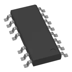
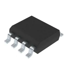
圖片僅供參考
NCP3064DR2G
IC REG BUCK BST ADJ 1.5A 8SOIC
- 製造商
- 製造商。 部分 #NCP3064DR2G
- 包 8-SOIC
- 資料表
- 有現貨的5457
100%原創; 新
24小時準備發貨
365天保修
RFQ&; 獲得更多折扣
規格
| Package | Tape & Reel (TR),Cut Tape (CT) |
| ProductStatus | Active |
| Function | Step-Up, Step-Down |
| OutputConfiguration | Positive or Negative |
| Topology | Buck, Boost |
| OutputType | Adjustable |
| NumberofOutputs | 1 |
| Voltage-Input(Min) | 3V |
| Voltage-Input(Max) | 40V |
| Voltage-Output(Min/Fixed) | 1.25V |
| Voltage-Output(Max) | 40V |
| Current-Output | 1.5A (Switch) |
| Frequency-Switching | 150kHz |
| SynchronousRectifier | No |
| OperatingTemperature | 0°C ~ 70°C (TJ) |
| MountingType | Surface Mount |
| Package/Case | 8-SOIC (0.154, 3.90mm Width) |
概述
Description
NCP3064DR2G is an On Semiconductor SMPS controller for flyback converters. It’s used in isolated power supplies such as offline adapters, chargers, and LED drivers. The device implements fixed‑frequency, current‑mode PWM to regulate energy transfer in a flyback transformer and typically drives an external MOSFET (external FET variants exist in related parts). It provides a startup/current‑source to power its VDD, a current‑sense/input, and a feedback input (via optocoupler or primary‑side regulation) to set duty cycle. Protection features usually include undervoltage lockout, overcurrent/short‑circuit protection, overvoltage protection, and thermal shutdown. The DR2G suffix denotes the specific RoHS/compliant package variant (8‑pin). In short, NCP3064DR2G is a compact controller designed to simplify design of compact, efficient isolated power supplies by handling PWM control and protection while requiring only a minimal external components around a flyback transformer. For exact electrical specs, pinout, and application guidelines, refer to the current NCP3064DR2G datasheet.
Package
NCP3064DR2G comes in an 8-pin SOIC (surface-mount) package.
Pinout
- Pin count: 8 pins (in an 8-pin SOIC/DIP package, code DR2G).
- Function: High-voltage, current‑mode PWM controller for offline flyback/switch‑mode power supplies. It regulates via primary current sense and feedback, includes oscillator timing (RT/CT), undervoltage/enable features, and drives the MOSFET gate (external or integrated depending on variant). Typical pins provide Vcc (supply), GND, FB (feedback), IS (current sense), RT/CT (timing), OUTPUT (gate drive), and HV input (DRAIN/VIN) for the primary side. For exact pinout, refer to the datasheet.
- Function: High-voltage, current‑mode PWM controller for offline flyback/switch‑mode power supplies. It regulates via primary current sense and feedback, includes oscillator timing (RT/CT), undervoltage/enable features, and drives the MOSFET gate (external or integrated depending on variant). Typical pins provide Vcc (supply), GND, FB (feedback), IS (current sense), RT/CT (timing), OUTPUT (gate drive), and HV input (DRAIN/VIN) for the primary side. For exact pinout, refer to the datasheet.
Manufacturer
- Manufacturer: ON Semiconductor (ON Semi).
- What kind of company: An American multinational semiconductor designer and manufacturer specializing in energy-efficient electronics, including power management, analog, sensors, and automotive ICs.
- What kind of company: An American multinational semiconductor designer and manufacturer specializing in energy-efficient electronics, including power management, analog, sensors, and automotive ICs.
Application
NCP3064DR2G is a high‑voltage, current‑mode PWM controller for off‑line flyback SMPS. Typical applications:
- AC/DC adapters and wall‑wart/brick power supplies
- Battery chargers
- Standby/auxiliary power supplies for consumer electronics (TVs, monitors, set‑top boxes)
- General low‑to‑medium power flyback SMPS designs
(Uses: fixed‑frequency flyback regulation in primary‑side controlled systems.)
- AC/DC adapters and wall‑wart/brick power supplies
- Battery chargers
- Standby/auxiliary power supplies for consumer electronics (TVs, monitors, set‑top boxes)
- General low‑to‑medium power flyback SMPS designs
(Uses: fixed‑frequency flyback regulation in primary‑side controlled systems.)
Equivalent
NCP3064DR2G is an ON Semiconductor high‑voltage, current‑mode PWM controller for flyback converters (offline). There isn’t an exact pin‑for‑pin replacement; closest functional equivalents include:
- ON Semiconductor: other NCP306x parts (e.g., NCP3063, NCP3065) for similar control
- TI: UC3842/UC3843/UC3844 (external FET, current‑mode PWM)
- ST: VIPER12A/VIPER22A (offline flyback with integrated FET)
- Power Integrations: TinySwitch‑II LNK3xx (integrated FET)
Note: check HV rating, startup current, frequency, and pinout for your design.
- ON Semiconductor: other NCP306x parts (e.g., NCP3063, NCP3065) for similar control
- TI: UC3842/UC3843/UC3844 (external FET, current‑mode PWM)
- ST: VIPER12A/VIPER22A (offline flyback with integrated FET)
- Power Integrations: TinySwitch‑II LNK3xx (integrated FET)
Note: check HV rating, startup current, frequency, and pinout for your design.
船舶
運輸管道我們
通過DHL、FedEx、TNT、UPS或您選擇的任何其他貨運代理提供全球運輸服務。
運費參攷(DHL/FedEx):
動態主要裝載: 運費從25美元到45美元(0.5公斤)不等,預計交貨時間為2-5個工作日。
聯邦快遞: 運費從25美元到40美元(0.5公斤)不等,預計交貨時間為3-7個工作日。
不斷電供應系統: 運費從25美元到45美元(0.5公斤)不等,預計交貨時間為3-7個工作日。
三硝基甲苯: 運費從25美元到65美元(0.5公斤)不等,預計交貨時間為3-7個工作日。
增强型短消息: 運費從30美元到50美元(0.5公斤)不等,預計交貨時間為7-15個工作日。
掛號: 運費為2-4美元(0.1公斤),預計交貨時間為5-20個工作日。
支付
Payment Methods
付款條件為100%預付。
現時,我們只接受以下付款方式:
1. 貝寶
2. 信用卡/借記卡
3. 電匯
類似的
-
![MX25V5126FM1I]() MX25V5126FM1I
Macronix
-
![MX25V4035FZUI]() MX25V4035FZUI
Macronix
-
![MX25R3235FZNIL0]() MX25R3235FZNIL0
Macronix
-
![MX25L8035EM2I-10G]() MX25L8035EM2I-10G
Macronix
-
![MX25L12833FM2I-10G]() MX25L12833FM2I-10..
Macronix
-
![MX25L12833FZ2I-10G]() MX25L12833FZ2I-10..
Macronix
-
![MX25U25645GXDI00]() MX25U25645GXDI00
Macronix
-
![MX29F800CBTI-70G]() MX29F800CBTI-70G
Macronix
-
![MX29LV640ETTI-70G]() MX29LV640ETTI-70G
Macronix
-
![MX25L25735FMI-10G]() MX25L25735FMI-10G
Macronix
-
![MX30LF4G18AC-TI]() MX30LF4G18AC-TI
Macronix
-
![MX25L1006EMI-10G]() MX25L1006EMI-10G
Macronix