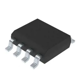
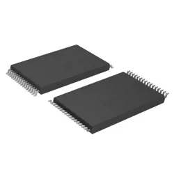
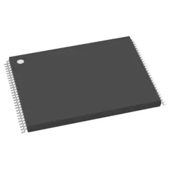
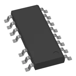
圖片僅供參考
NB3N551DG
IC CLK BUFFER 1:4 180MHZ 8SOIC
- 製造商
- 製造商。 部分 #NB3N551DG
- 包
- 資料表
- 有現貨的8809
100%原創; 新
24小時準備發貨
365天保修
RFQ&; 獲得更多折扣
規格
| Part Status | Obsolete |
| Type | Fanout Buffer (Distribution) |
| Number of Circuits | 1 |
| Ratio - Input:Output | 1:4 |
| Differential - Input:Output | No/No |
| Input | LVCMOS, LVTTL |
| Output | LVCMOS, LVTTL |
| Frequency - Max | 180 MHz |
| Voltage - Supply | 3V ~ 5.5V |
| Operating Temperature | -40°C ~ 85°C |
| Mounting Type | Surface Mount |
| Package / Case | 8-SOIC (0.154", 3.90mm Width) |
| Supplier Device Package | 8-SOIC |
| Base Product Number | NB3N551 |
概述
Description
The NB3N551DG is a high-performance clock buffer and fanout device designed primarily for applications requiring precise timing and signal integrity. It operates by distributing a single clock input to multiple outputs, ensuring that the timing signals remain synchronized and stable across various components in a system.
Key features of the NB3N551DG include low propagation delay, low jitter, and high drive capability, making it suitable for high-speed digital circuits. It typically supports differential clock inputs and offers multiple single-ended clock outputs, facilitating flexibility in design. The device is commonly used in telecommunications, computing, and data processing systems where maintaining signal integrity across multiple loads is critical.
Additionally, the NB3N551DG often comes in a compact package, making it suitable for space-constrained applications. Designers favor this device for its reliability and performance in distributing clock signals across various components in complex electronic systems.
Features
The NB3N551DG is a high-performance, low-skew, 1-to-4 clock buffer designed for use in high-speed digital applications. Key features include:
1. Input Compatibility: It supports both LVCMOS and LVTTL input levels, making it versatile for various systems.
2. Low Skew: Provides low output-to-output skew, ensuring minimal timing discrepancies across outputs, which is critical for synchronous operations.
3. High Drive Capability: Capable of driving large capacitive loads, suitable for high fan-out applications.
4. Power Supply Range: Operates over a wide supply voltage range, enhancing its applicability in different systems.
5. Temperature Range: Designed to function effectively across a broad temperature range, suitable for industrial applications.
6. Small Package: Available in a compact package, facilitating space-saving designs in PCB layouts.
These features make the NB3N551DG ideal for use in clock distribution networks, data communications, and general timing applications in various electronic devices.
Package
The NB3N551DG is packaged in a 5-pin SOT-23 (Small Outline Transistor) package. This surface-mount package is compact and suitable for various applications in electronics.
Pinout
The NB3N551DG is a versatile clock driver from ON Semiconductor, specifically designed for high-performance applications. It features a pin count of 16 pins.
The primary functions of the NB3N551DG include:
1. Input/Output: It has differential inputs for receiving clock signals and multiple outputs for distributing the clock.
2. Clock Distribution: It is capable of buffering and distributing high-speed clock signals with low skew and minimal jitter.
3. Voltage Levels: It operates with a wide supply voltage range, accommodating different system requirements.
4. Enable/Disable Control: The device includes an enable pin to control output activity, ensuring power efficiency.
The NB3N551DG is widely utilized in applications such as telecommunications, data processing, and high-speed digital systems.
Manufacturer
The NB3N551DG is manufactured by ON Semiconductor, a global supplier of semiconductor-based solutions. ON Semiconductor specializes in a wide range of products including power management, analog, sensors, and logic devices. The company serves various industries such as automotive, communications, computing, consumer electronics, and industrial applications. Headquartered in Phoenix, Arizona, ON Semiconductor focuses on providing efficient and innovative solutions to meet the demands of modern electronic systems.
Application
The NB3N551DG is a high-speed voltage-level translator commonly used in applications such as data communication, signal conditioning, and interfacing between devices operating at different voltage levels. It is ideal for interfacing I2C, SPI, and UART protocols in mixed-voltage systems, commonly found in consumer electronics, automotive, and industrial applications. Additionally, it assists in connecting microcontrollers, sensors, and other peripherals with varying logic levels efficiently.
Equivalent
The NB3N551DG chip is typically equivalent to other buffer or translator chips such as the SN74LVTH16245, MC74LCX16245, or similar devices in terms of functionality. However, specific equivalents can vary based on voltage levels, speed, and application requirements. Always check the datasheets for detailed specifications to ensure compatibility.
船舶
運輸管道我們
通過DHL、FedEx、TNT、UPS或您選擇的任何其他貨運代理提供全球運輸服務。
運費參攷(DHL/FedEx):
動態主要裝載: 運費從25美元到45美元(0.5公斤)不等,預計交貨時間為2-5個工作日。
聯邦快遞: 運費從25美元到40美元(0.5公斤)不等,預計交貨時間為3-7個工作日。
不斷電供應系統: 運費從25美元到45美元(0.5公斤)不等,預計交貨時間為3-7個工作日。
三硝基甲苯: 運費從25美元到65美元(0.5公斤)不等,預計交貨時間為3-7個工作日。
增强型短消息: 運費從30美元到50美元(0.5公斤)不等,預計交貨時間為7-15個工作日。
掛號: 運費為2-4美元(0.1公斤),預計交貨時間為5-20個工作日。
支付
Payment Methods
付款條件為100%預付。
現時,我們只接受以下付款方式:
1. 貝寶
2. 信用卡/借記卡
3. 電匯
類似的
-
![MX29F400CBTI-70G]() MX29F400CBTI-70G
Macronix
-
![MX66U1G45GXDI00]() MX66U1G45GXDI00
Macronix
-
![MX25V4035FZUI]() MX25V4035FZUI
Macronix
-
![MX29GL512FHXFI-11G]() MX29GL512FHXFI-11..
Macronix
-
![MX25U51279GXDR00]() MX25U51279GXDR00
Macronix
-
![MX25V1635FM2I]() MX25V1635FM2I
Macronix
-
![MX25U6435FM2I-10G]() MX25U6435FM2I-10G
Macronix
-
![MX25U25645GXDI00]() MX25U25645GXDI00
Macronix
-
![MX25L12835FZ2I-10G]() MX25L12835FZ2I-10..
Macronix
-
![MX29F040CTI-70G]() MX29F040CTI-70G
Macronix
-
![MX29LV640ETTI-70G]() MX29LV640ETTI-70G
Macronix
-
![MX25L25735FMI-10G]() MX25L25735FMI-10G
Macronix