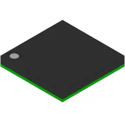
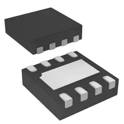
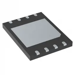
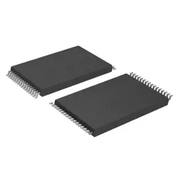
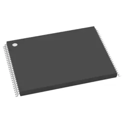
圖片僅供參考
MX29LV040CQI-70G
IC FLASH 4MBIT PARALLEL 32PLCC
- 製造商
- 製造商。 部分 #MX29LV040CQI-70G
- 包
- 資料表
- 有現貨的4538
100%原創; 新
24小時準備發貨
365天保修
RFQ&; 獲得更多折扣
規格
| Series | MX29LV |
| Part Status | Obsolete |
| Base Product Number | MX29LV040 |
| DigiKey Programmable | Not Verified |
| Memory Type | Non-Volatile |
| Memory Format | FLASH |
| Technology | FLASH - NOR |
| Memory Size | 4Mbit |
| Memory Organization | 512K x 8 |
| Memory Interface | Parallel |
| Write Cycle Time - Word, Page | 70ns |
| Voltage - Supply | 2.7V ~ 3.6V |
| Operating Temperature | -40°C ~ 85°C (TA) |
| Mounting Type | Surface Mount |
| Package | 32-LCC (J-Lead) |
| Supplier Device Package | 32-PLCC (11.43x14.05) |
| Packaging | Tray |
| Access Time | 70 ns |
概述
Description
The MX29LV040CQI-70G is a CMOS Flash memory chip designed for versatile applications, including embedded systems and consumer electronics. It features a 4 Megabit (512K x 8) memory capacity, allowing for storage of firmware, configurations, and other data. The "70G" in its name indicates a maximum access time of 70 nanoseconds, making it suitable for high-speed operations.
This chip utilizes a standard 32-pin TSOP (Thin Small Outline Package) and supports both parallel and serial programming interfaces. It has a wide voltage range (typically 3V to 3.6V), enabling compatibility with various devices. The MX29LV040CQI-70G supports multiple read, erase, and program cycles, ensuring reliability and efficiency in data management.
Key features include fast read speeds, low power consumption, and the ability to perform sector or bulk erase operations. With its robust performance and reliability, the MX29LV040CQI-70G is ideal for applications in telecommunications, automotive, and industrial control systems.
This chip utilizes a standard 32-pin TSOP (Thin Small Outline Package) and supports both parallel and serial programming interfaces. It has a wide voltage range (typically 3V to 3.6V), enabling compatibility with various devices. The MX29LV040CQI-70G supports multiple read, erase, and program cycles, ensuring reliability and efficiency in data management.
Key features include fast read speeds, low power consumption, and the ability to perform sector or bulk erase operations. With its robust performance and reliability, the MX29LV040CQI-70G is ideal for applications in telecommunications, automotive, and industrial control systems.
Features
The MX29LV040CQI-70G is a 4 Mbit (512K x 8) flash memory device from Macronix, designed for embedded applications. Key features include:
1. Technology: Uses CMOS technology for low power consumption.
2. Interface: Provides an 8-bit parallel I/O interface for data transfer.
3. Access Speed: Offers a maximum access time of 70 ns.
4. Programming Voltage: Operates at 3.0V to 3.6V for read and programming, ensuring compatibility with low-voltage systems.
5. Erase Capability: Supports sector erase and chip erase functions, with a typical erase time of 0.5 seconds per sector.
6. Endurance: Designed for a minimum of 100,000 program/erase cycles per sector.
7. Data Retention: Ensures data retention of over 20 years.
8. Package: Available in a 32-pin SOP (Small Outline Package) for space-efficient design.
These features make the MX29LV040CQI-70G suitable for applications in consumer electronics, telecommunications, and automotive systems.
1. Technology: Uses CMOS technology for low power consumption.
2. Interface: Provides an 8-bit parallel I/O interface for data transfer.
3. Access Speed: Offers a maximum access time of 70 ns.
4. Programming Voltage: Operates at 3.0V to 3.6V for read and programming, ensuring compatibility with low-voltage systems.
5. Erase Capability: Supports sector erase and chip erase functions, with a typical erase time of 0.5 seconds per sector.
6. Endurance: Designed for a minimum of 100,000 program/erase cycles per sector.
7. Data Retention: Ensures data retention of over 20 years.
8. Package: Available in a 32-pin SOP (Small Outline Package) for space-efficient design.
These features make the MX29LV040CQI-70G suitable for applications in consumer electronics, telecommunications, and automotive systems.
Package
The MX29LV040CQI-70G is typically packaged in a 32-pin TSOP (Thin Small Outline Package) format. This package type is designed for space efficiency and is commonly used in memory devices.
Pinout
The MX29LV040CQI-70G is a 4Mb (512K x 8) flash memory device with a pin count of 32.
Pin Functionality:
1. Address Pins (A0-A18): Used for addressing the memory locations.
2. Data Pins (DQ0-DQ7): 8-bit data input/output.
3. Chip Enable (CE): Activates the memory chip.
4. Output Enable (OE): Enables data output.
5. Write Enable (WE): Controls write operations.
6. Reset (RESET): Resets the internal state.
7. Common Ground (VSS): Ground reference.
8. Power Supply (VCC): Positive power supply for operation.
9. RMV (Ready/Busy): Indicates the status of read/write operations.
This device operates at a maximum access time of 70 ns and supports multiple read and write cycles, making it suitable for various applications in embedded systems.
Pin Functionality:
1. Address Pins (A0-A18): Used for addressing the memory locations.
2. Data Pins (DQ0-DQ7): 8-bit data input/output.
3. Chip Enable (CE): Activates the memory chip.
4. Output Enable (OE): Enables data output.
5. Write Enable (WE): Controls write operations.
6. Reset (RESET): Resets the internal state.
7. Common Ground (VSS): Ground reference.
8. Power Supply (VCC): Positive power supply for operation.
9. RMV (Ready/Busy): Indicates the status of read/write operations.
This device operates at a maximum access time of 70 ns and supports multiple read and write cycles, making it suitable for various applications in embedded systems.
Manufacturer
The MX29LV040CQI-70G is manufactured by Macronix International Co., Ltd. Macronix is a semiconductor company based in Taiwan, specializing in non-volatile memory solutions, including NOR Flash and NAND Flash memory products. Founded in 1989, the company focuses on providing high-performance memory devices for a variety of applications, such as consumer electronics, automotive, and industrial sectors. Macronix is known for its commitment to quality and innovation in memory technology.
Application
The MX29LV040CQI-70G is a 4 Mb (512 K x 8) flash memory chip commonly used in applications such as embedded systems, consumer electronics, automotive electronics, telecommunications equipment, and industrial controls. It serves for code storage, firmware updates, and data retention in devices like routers, set-top boxes, and programmable logic controllers (PLCs). Its low power consumption and fast read speeds make it suitable for diverse applications requiring non-volatile storage.
Equivalent
The MX29LV040CQI-70G is a 4Mb (512KB x 8) Flash memory chip. Equivalent products include:
1. Am29F040B - AMD
2. W29C040 - Winbond
3. S29GL040A - Spansion
4. AT49F040 - Atmel
These alternatives feature similar specifications, such as data width and access times. Always check specific compatibility for your application.
1. Am29F040B - AMD
2. W29C040 - Winbond
3. S29GL040A - Spansion
4. AT49F040 - Atmel
These alternatives feature similar specifications, such as data width and access times. Always check specific compatibility for your application.
船舶
運輸管道我們
通過DHL、FedEx、TNT、UPS或您選擇的任何其他貨運代理提供全球運輸服務。
運費參攷(DHL/FedEx):
動態主要裝載: 運費從25美元到45美元(0.5公斤)不等,預計交貨時間為2-5個工作日。
聯邦快遞: 運費從25美元到40美元(0.5公斤)不等,預計交貨時間為3-7個工作日。
不斷電供應系統: 運費從25美元到45美元(0.5公斤)不等,預計交貨時間為3-7個工作日。
三硝基甲苯: 運費從25美元到65美元(0.5公斤)不等,預計交貨時間為3-7個工作日。
增强型短消息: 運費從30美元到50美元(0.5公斤)不等,預計交貨時間為7-15個工作日。
掛號: 運費為2-4美元(0.1公斤),預計交貨時間為5-20個工作日。
支付
Payment Methods
付款條件為100%預付。
現時,我們只接受以下付款方式:
1. 貝寶
2. 信用卡/借記卡
3. 電匯
類似的
-
![MX25L3233FZBI-08Q]() MX25L3233FZBI-08Q
MX25L3233FZBI-08Q
Macronix
-
![MX25V1635FZNQ03]() MX25V1635FZNQ03
MX25V1635FZNQ03
Macronix
-
![MX25V5126FM1I]() MX25V5126FM1I
MX25V5126FM1I
Macronix
-
![MX25V16066M2I02]() MX25V16066M2I02
MX25V16066M2I02
Macronix
-
![MX25L25673GMI-08G]() MX25L25673GMI-08G
MX25L25673GMI-08G
Macronix
-
![MX29GL512FHXFI-11G]() MX29GL512FHXFI-11..
MX29GL512FHXFI-11..
Macronix
-
![MX25U3232FZBI02]() MX25U3232FZBI02
MX25U3232FZBI02
Macronix
-
![MX25L12833FM2I-10G]() MX25L12833FM2I-10..
MX25L12833FM2I-10..
Macronix
-
![MX25U25645GXDI00]() MX25U25645GXDI00
MX25U25645GXDI00
Macronix
-
![MX25L12835FZ2I-10G]() MX25L12835FZ2I-10..
MX25L12835FZ2I-10..
Macronix
-
![MX29F040CTI-70G]() MX29F040CTI-70G
MX29F040CTI-70G
Macronix
-
![MX29F800CBTI-70G]() MX29F800CBTI-70G
MX29F800CBTI-70G
Macronix