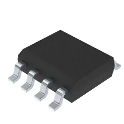
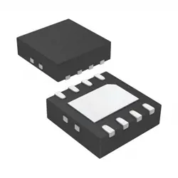
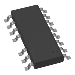
圖片僅供參考
LTC1689IS
RS-485 Interface IC LTC1689 - 100Mbps RS485 Hot Swapable Quad Drivers
- 製造商
- 製造商。 部分 #LTC1689IS
- 包
- 資料表 LTC1689IS DataSheet
- 有現貨的15814
100%原創; 新
24小時準備發貨
365天保修
RFQ&; 獲得更多折扣
規格
概述
Description
The LTC1689IS is a high-speed, low-power, 12-bit analog-to-digital converter (ADC) designed for a variety of precision applications, including medical instrumentation, data acquisition, and industrial control. It operates with a sample rate of up to 1 MSPS and features a differential input, providing excellent noise immunity and improved accuracy.
The device includes an internal reference, simplifying design and integration, and supports both single-ended and differential input configurations. With a low power consumption of typically 15 mW, the LTC1689IS is suitable for battery-powered applications.
Its serial SPI-compatible interface allows for easy interfacing with microcontrollers and digital signal processors, enabling seamless data transfer. The LTC1689IS also incorporates features such as adjustable gain and offset correction, enhancing measurement precision.
Overall, the LTC1689IS is ideal for applications requiring high-resolution data conversion with low power and high speed.
The device includes an internal reference, simplifying design and integration, and supports both single-ended and differential input configurations. With a low power consumption of typically 15 mW, the LTC1689IS is suitable for battery-powered applications.
Its serial SPI-compatible interface allows for easy interfacing with microcontrollers and digital signal processors, enabling seamless data transfer. The LTC1689IS also incorporates features such as adjustable gain and offset correction, enhancing measurement precision.
Overall, the LTC1689IS is ideal for applications requiring high-resolution data conversion with low power and high speed.
Features
The LTC1689IS is a high-speed, low-power, 16-bit analog-to-digital converter (ADC) designed for precision data acquisition applications. Key features include:
1. Sampling Rate: Up to 1 MSPS (mega samples per second).
2. Resolution: 16 bits, enabling high precision in measurements.
3. Input Range: Supports a wide input voltage range, including single-ended and differential inputs.
4. Low Power Consumption: Operates at low power levels, making it suitable for battery-operated devices.
5. Integrated Reference: Features an internal reference voltage, simplifying design and reducing component count.
6. Fast Settling Time: Quick settling time allows for efficient sampling of rapidly changing signals.
7. Parallel or Serial Output: Offers flexibility in data output formats, accommodating various system designs.
8. Built-in Sample-and-Hold: Ensures accurate conversion of dynamic signals.
9. Temperature Range: Typically specified for industrial temperature ranges, enhancing reliability in various environments.
Overall, the LTC1689IS is ideal for applications in medical instrumentation, industrial monitoring, and portable data acquisition systems.
1. Sampling Rate: Up to 1 MSPS (mega samples per second).
2. Resolution: 16 bits, enabling high precision in measurements.
3. Input Range: Supports a wide input voltage range, including single-ended and differential inputs.
4. Low Power Consumption: Operates at low power levels, making it suitable for battery-operated devices.
5. Integrated Reference: Features an internal reference voltage, simplifying design and reducing component count.
6. Fast Settling Time: Quick settling time allows for efficient sampling of rapidly changing signals.
7. Parallel or Serial Output: Offers flexibility in data output formats, accommodating various system designs.
8. Built-in Sample-and-Hold: Ensures accurate conversion of dynamic signals.
9. Temperature Range: Typically specified for industrial temperature ranges, enhancing reliability in various environments.
Overall, the LTC1689IS is ideal for applications in medical instrumentation, industrial monitoring, and portable data acquisition systems.
Package
The LTC1689IS is available in a 16-lead TSSOP (Thin Shrink Small Outline Package) package type.
Pinout
The LTC1689IS is a high-speed, high-accuracy, 10-bit digital-to-analog converter (DAC) from Analog Devices. It features a 20-pin TSSOP package. The primary function of the LTC1689IS is to convert digital signals into corresponding analog voltages with precision and speed, making it suitable for applications in control systems, signal generation, and instrumentation.
Key pin functions include:
1. Data Input (DB0-DB9): Digital data input (10 bits).
2. Clock (CLK): Synchronizes data input.
3. Load (LD): Loads the input data into the DAC.
4. Reference Voltage (VREF): Sets the output voltage range.
5. Output Voltage (VOUT): The analog output.
6. Power Supply (VDD): Supplies power to the device.
7. Ground (GND): Common ground connection.
The LTC1689IS offers low power consumption and high linearity, making it ideal for precision applications.
Key pin functions include:
1. Data Input (DB0-DB9): Digital data input (10 bits).
2. Clock (CLK): Synchronizes data input.
3. Load (LD): Loads the input data into the DAC.
4. Reference Voltage (VREF): Sets the output voltage range.
5. Output Voltage (VOUT): The analog output.
6. Power Supply (VDD): Supplies power to the device.
7. Ground (GND): Common ground connection.
The LTC1689IS offers low power consumption and high linearity, making it ideal for precision applications.
Manufacturer
The LTC1689IS is manufactured by Analog Devices, Inc., a prominent company in the semiconductor industry. Analog Devices specializes in designing and manufacturing high-performance analog, mixed-signal, and digital signal processing (DSP) integrated circuits (ICs). The company serves various markets, including communications, automotive, industrial, and consumer electronics, providing solutions for data conversion, signal processing, and power management. Founded in 1965, Analog Devices has established itself as a leader in precision analog technology, offering innovative products that enhance performance and efficiency in electronic systems.
Application
The LTC1689IS is a high-speed, low-power analog-to-digital converter (ADC) primarily used in applications such as portable instrumentation, data acquisition systems, medical imaging, industrial process control, and telecommunications. Its features make it suitable for applications requiring high resolution and fast conversion rates, including remote sensing, audio processing, and automotive sensor interfaces.
Equivalent
Equivalent products to the LTC1689IS include the Analog Devices AD7980, Texas Instruments ADS7894, and Microchip MCP3421. These alternatives may vary in specifications like resolution, sampling rate, and interface type, so it's essential to compare datasheets for specific application requirements.
船舶
運輸管道我們
通過DHL、FedEx、TNT、UPS或您選擇的任何其他貨運代理提供全球運輸服務。
運費參攷(DHL/FedEx):
動態主要裝載: 運費從25美元到45美元(0.5公斤)不等,預計交貨時間為2-5個工作日。
聯邦快遞: 運費從25美元到40美元(0.5公斤)不等,預計交貨時間為3-7個工作日。
不斷電供應系統: 運費從25美元到45美元(0.5公斤)不等,預計交貨時間為3-7個工作日。
三硝基甲苯: 運費從25美元到65美元(0.5公斤)不等,預計交貨時間為3-7個工作日。
增强型短消息: 運費從30美元到50美元(0.5公斤)不等,預計交貨時間為7-15個工作日。
掛號: 運費為2-4美元(0.1公斤),預計交貨時間為5-20個工作日。
支付
Payment Methods
付款條件為100%預付。
現時,我們只接受以下付款方式:
1. 貝寶
2. 信用卡/借記卡
3. 電匯
類似的
-
![MX25R8035FM1IL0]() MX25R8035FM1IL0
MX25R8035FM1IL0
Macronix
-
![MX29F400CBTI-70G]() MX29F400CBTI-70G
MX29F400CBTI-70G
Macronix
-
![MX25R3235FZNIL0]() MX25R3235FZNIL0
MX25R3235FZNIL0
Macronix
-
![MX30LF2G28AD-TI]() MX30LF2G28AD-TI
MX30LF2G28AD-TI
Macronix
-
![MX25L25673GMI-08G]() MX25L25673GMI-08G
MX25L25673GMI-08G
Macronix
-
![MX25U25643GZNI00]() MX25U25643GZNI00
MX25U25643GZNI00
Macronix
-
![MX25L2006EM1I-12G]() MX25L2006EM1I-12G
MX25L2006EM1I-12G
Macronix
-
![MX25V1635FM2I]() MX25V1635FM2I
MX25V1635FM2I
Macronix
-
![MX25L12833FZNI-10G]() MX25L12833FZNI-10..
MX25L12833FZNI-10..
Macronix
-
![MX25U25645GXDI00]() MX25U25645GXDI00
MX25U25645GXDI00
Macronix
-
![MX29LV160DTTI-70G]() MX29LV160DTTI-70G
MX29LV160DTTI-70G
Macronix
-
![MX25L25735FMI-10G]() MX25L25735FMI-10G
MX25L25735FMI-10G
Macronix