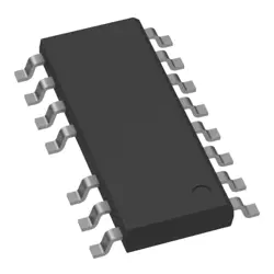
圖片僅供參考
LM2663M
IC REG CHARGE PUMP INV 8SOIC
- 製造商
- 製造商。 部分 #LM2663M
- 包 SOIC-8
- 資料表
- 有現貨的5448
100%原創; 新
24小時準備發貨
365天保修
RFQ&; 獲得更多折扣
規格
| Package | Tube |
| ProductStatus | Not For New Designs |
| Function | Ratiometric |
| OutputConfiguration | Positive or Negative |
| Topology | Charge Pump |
| OutputType | Fixed |
| NumberofOutputs | 1 |
| Voltage-Input(Min) | 1.5V |
| Voltage-Input(Max) | 5.5V |
| Voltage-Output(Min/Fixed) | -Vin, 2Vin, Vin/2 |
| Current-Output | 200mA |
| Frequency-Switching | 10kHz, 75kHz |
| SynchronousRectifier | No |
| OperatingTemperature | -40°C ~ 85°C (TA) |
| MountingType | Surface Mount |
| Package/Case | 8-SOIC (0.154, 3.90mm Width) |
概述
Description
The LM2663M is a charge pump voltage inverter integrated circuit (IC) primarily used for voltage conversion applications. It is commonly employed to generate a negative voltage from a positive supply, making it ideal for dual-supply systems where a negative voltage rail is needed. The device is part of the LM266x family from Texas Instruments known for its high efficiency and ease of use.
Key features of the LM2663M include:
1. Voltage Range: It operates over a wide input voltage range, typically from 1.5V to 5.5V.
2. Output Capability: The IC can produce a negative output voltage that is the inverse of the input voltage, up to a specified current limit.
3. Efficiency: It provides efficient operation with minimal power loss due to its capacitive charge pump design.
4. Frequency: The device operates at a fixed frequency, ensuring predictable performance and allowing for easy filtering.
5. Compact Design: It is available in a small form factor, making it suitable for space-constrained applications.
The LM2663M is commonly used in battery-powered devices, operational amplifiers, and other applications requiring a negative voltage supply.
Key features of the LM2663M include:
1. Voltage Range: It operates over a wide input voltage range, typically from 1.5V to 5.5V.
2. Output Capability: The IC can produce a negative output voltage that is the inverse of the input voltage, up to a specified current limit.
3. Efficiency: It provides efficient operation with minimal power loss due to its capacitive charge pump design.
4. Frequency: The device operates at a fixed frequency, ensuring predictable performance and allowing for easy filtering.
5. Compact Design: It is available in a small form factor, making it suitable for space-constrained applications.
The LM2663M is commonly used in battery-powered devices, operational amplifiers, and other applications requiring a negative voltage supply.
Features
The LM2663M is a charge pump voltage inverter with several key features:
1. Voltage Inversion: Converts a positive input voltage to a negative output voltage.
2. Input Voltage Range: Operates with input voltages from 1.5V to 5.5V.
3. Output Voltage: Provides a negative output voltage approximately equal to the magnitude of the input voltage.
4. Output Current: Capable of supplying up to 200 mA of output current.
5. Efficiency: High efficiency with a typical conversion efficiency of 90% to 95%.
6. Low Quiescent Current: Consumes minimal quiescent current, typically around 300 μA, which is crucial for battery-powered applications.
7. Shutdown Mode: Includes a shutdown mode that reduces the supply current to less than 1 μA, enhancing power savings.
8. Compact Package: Available in a small 8-pin SOIC (Small Outline Integrated Circuit) package, suitable for space-constrained designs.
9. Wide Temperature Range: Operates in a temperature range from -40°C to +85°C, making it suitable for industrial applications.
10. Minimal External Components: Requires only a few external capacitors for operation, simplifying the design process.
These features make the LM2663M ideal for applications requiring efficient voltage inversion in compact and low-power designs.
1. Voltage Inversion: Converts a positive input voltage to a negative output voltage.
2. Input Voltage Range: Operates with input voltages from 1.5V to 5.5V.
3. Output Voltage: Provides a negative output voltage approximately equal to the magnitude of the input voltage.
4. Output Current: Capable of supplying up to 200 mA of output current.
5. Efficiency: High efficiency with a typical conversion efficiency of 90% to 95%.
6. Low Quiescent Current: Consumes minimal quiescent current, typically around 300 μA, which is crucial for battery-powered applications.
7. Shutdown Mode: Includes a shutdown mode that reduces the supply current to less than 1 μA, enhancing power savings.
8. Compact Package: Available in a small 8-pin SOIC (Small Outline Integrated Circuit) package, suitable for space-constrained designs.
9. Wide Temperature Range: Operates in a temperature range from -40°C to +85°C, making it suitable for industrial applications.
10. Minimal External Components: Requires only a few external capacitors for operation, simplifying the design process.
These features make the LM2663M ideal for applications requiring efficient voltage inversion in compact and low-power designs.
Package
The LM2663M is available in an 8-pin SOIC (Small Outline Integrated Circuit) package.
Pinout
The LM2663M is a charge pump voltage converter IC that has 8 pins. It is designed for voltage inversion and voltage doubling applications. Here's a brief overview of its pin functions:
1. Pin 1 (CAP+): Connects to the positive terminal of the flying capacitor.
2. Pin 2 (GND): Ground connection.
3. Pin 3 (CAP-): Connects to the negative terminal of the flying capacitor.
4. Pin 4 (OUT): Output voltage pin, which provides the inverted or doubled voltage.
5. Pin 5 (LV): Low-voltage operation mode pin. It is used to enable or disable the low-voltage feature.
6. Pin 6 (SHDN): Shutdown pin. Active-low input used to disable the device and reduce power consumption.
7. Pin 7 (VIN): Power supply input voltage pin.
8. Pin 8 (FB): Feedback pin for voltage regulation, typically used for voltage doubling applications.
This IC is particularly useful in applications requiring negative voltage generation from a positive input supply or doubling the input voltage.
1. Pin 1 (CAP+): Connects to the positive terminal of the flying capacitor.
2. Pin 2 (GND): Ground connection.
3. Pin 3 (CAP-): Connects to the negative terminal of the flying capacitor.
4. Pin 4 (OUT): Output voltage pin, which provides the inverted or doubled voltage.
5. Pin 5 (LV): Low-voltage operation mode pin. It is used to enable or disable the low-voltage feature.
6. Pin 6 (SHDN): Shutdown pin. Active-low input used to disable the device and reduce power consumption.
7. Pin 7 (VIN): Power supply input voltage pin.
8. Pin 8 (FB): Feedback pin for voltage regulation, typically used for voltage doubling applications.
This IC is particularly useful in applications requiring negative voltage generation from a positive input supply or doubling the input voltage.
Manufacturer
The LM2663M is manufactured by Texas Instruments. Texas Instruments, often abbreviated as TI, is an American technology company renowned for designing and manufacturing semiconductors and various integrated circuits, which it sells to electronics designers and manufacturers globally. TI is one of the largest semiconductor companies in the world and is particularly well-known for its analog chips and embedded processors. The company caters to a wide range of industries, including automotive, industrial, personal electronics, and communications equipment. Texas Instruments is headquartered in Dallas, Texas, and has a significant presence worldwide, with operations in more than 30 countries.
Application
The LM2663M is a switched capacitor voltage converter primarily used in applications requiring voltage inversion or doubling. Common areas of application include powering analog and digital circuits from a single supply, generating negative voltages for operational amplifiers, and battery-powered devices needing dual supply voltages. It's also used in portable electronics, voltage biasing, and signal processing where efficient low-power conversion is needed.
Equivalent
The LM2663M is a charge pump voltage inverter. Equivalent products include the TPS60403 from Texas Instruments, the MAX660 from Maxim Integrated, the ADM8660 from Analog Devices, and the LTC660 from Linear Technology. These components offer similar voltage inversion capabilities, but be sure to check specific parameters such as input voltage range, output current, switching frequency, and efficiency to ensure compatibility with your application.
船舶
運輸管道我們
通過DHL、FedEx、TNT、UPS或您選擇的任何其他貨運代理提供全球運輸服務。
運費參攷(DHL/FedEx):
動態主要裝載: 運費從25美元到45美元(0.5公斤)不等,預計交貨時間為2-5個工作日。
聯邦快遞: 運費從25美元到40美元(0.5公斤)不等,預計交貨時間為3-7個工作日。
不斷電供應系統: 運費從25美元到45美元(0.5公斤)不等,預計交貨時間為3-7個工作日。
三硝基甲苯: 運費從25美元到65美元(0.5公斤)不等,預計交貨時間為3-7個工作日。
增强型短消息: 運費從30美元到50美元(0.5公斤)不等,預計交貨時間為7-15個工作日。
掛號: 運費為2-4美元(0.1公斤),預計交貨時間為5-20個工作日。
支付
Payment Methods
付款條件為100%預付。
現時,我們只接受以下付款方式:
1. 貝寶
2. 信用卡/借記卡
3. 電匯
類似的
-
![MX25L3233FZBI-08Q]() MX25L3233FZBI-08Q
Macronix
-
![MX25L3233FM1I-08Q]() MX25L3233FM1I-08Q
Macronix
-
![MX25V16066M2I02]() MX25V16066M2I02
Macronix
-
![MX25L25673GMI-08G]() MX25L25673GMI-08G
Macronix
-
![MX25U51279GXDR00]() MX25U51279GXDR00
Macronix
-
![MX25U25643GZNI00]() MX25U25643GZNI00
Macronix
-
![MX25L2006EM1I-12G]() MX25L2006EM1I-12G
Macronix
-
![MX25U6435FM2I-10G]() MX25U6435FM2I-10G
Macronix
-
![MX25L12833FM2I-10G]() MX25L12833FM2I-10..
Macronix
-
![MX25L12835FZ2I-10G]() MX25L12835FZ2I-10..
Macronix
-
![MX25L25645GXDI-08G]() MX25L25645GXDI-08..
Macronix
-
![MX25L25735FMI-10G]() MX25L25735FMI-10G
Macronix