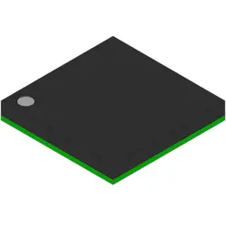
圖片僅供參考
LFE3-70EA-6FN484I
IC FPGA 295 I/O 484FBGA
- 製造商
- 製造商。 部分 #LFE3-70EA-6FN484I
- 包 484-BBGA
- 資料表 LFE3-70EA-6FN484I DataSheet
- 有現貨的9680
100%原創; 新
24小時準備發貨
365天保修
RFQ&; 獲得更多折扣
規格
| Supplier | Lattice Semiconductor Corporation |
| Package | Tray |
| Series | ECP3 |
| ProductStatus | Active |
| NumberofLABs/CLBs | 8375 |
| NumberofLogicElements/Cells | 67000 |
| TotalRAMBits | 4526080 |
| NumberofI/O | 295 |
| Voltage-Supply | 1.14V ~ 1.26V |
| MountingType | Surface Mount |
| OperatingTemperature | -40°C ~ 100°C (TJ) |
| Package/Case | 484-BBGA |
概述
Description
Introduction to LFE3-70EA-6FN484I
- What it is: A high-density FPGA from Lattice Semiconductor, part of the LFE3 family.
- Package and temperature: 484-ball fine-pitch BGA (FN484), industrial temperature range (I).
- Capacity and naming: roughly tens of thousands of logic elements (the “70” hints at about 70k LE capacity); contains RAM blocks, DSP blocks/MAC, PLLs, and configurable I/O.
- I/O and design resources: multiple I/O banks supporting various standards; on-chip memory and DSP resources for signal processing and logic-intensive tasks.
- Development flow: designed with Lattice Diamond or Radiant toolchains; bitstream generated and programmed via Lattice programmers (JTAG/SPI options available).
- Typical applications: digital signal processing, image/video processing, communications, embedded control, instrumentation, and other dense logic/IP-heavy designs.
- How to verify details: consult the official Lattice datasheet for exact counts (LEs, RAM, DSP blocks, I/O, transceivers), timing, and package pinout.
Note: Exact resource counts vary; always check the datasheet for precise specifications.
- What it is: A high-density FPGA from Lattice Semiconductor, part of the LFE3 family.
- Package and temperature: 484-ball fine-pitch BGA (FN484), industrial temperature range (I).
- Capacity and naming: roughly tens of thousands of logic elements (the “70” hints at about 70k LE capacity); contains RAM blocks, DSP blocks/MAC, PLLs, and configurable I/O.
- I/O and design resources: multiple I/O banks supporting various standards; on-chip memory and DSP resources for signal processing and logic-intensive tasks.
- Development flow: designed with Lattice Diamond or Radiant toolchains; bitstream generated and programmed via Lattice programmers (JTAG/SPI options available).
- Typical applications: digital signal processing, image/video processing, communications, embedded control, instrumentation, and other dense logic/IP-heavy designs.
- How to verify details: consult the official Lattice datasheet for exact counts (LEs, RAM, DSP blocks, I/O, transceivers), timing, and package pinout.
Note: Exact resource counts vary; always check the datasheet for precise specifications.
Features
Here are concise features of LFE3-70EA-6FN484I:
- FPGA family: LFE3
- Logic elements: ~70K LEs
- Package: 484-pin Fine-PBGA (FN484)
- Speed grade: -6
- Memory: Block RAM plus distributed RAM
- DSP: DSP/multiplier blocks for MAC operations
- Clocking: PLLs for flexible clock generation and distribution
- I/O: Multiple I/O banks with broad voltage/standards support; numerous I/O pins
- Configuration/Debug: JTAG, SPI/config options; boundary-scan and on-chip debugging
- Power:typical low-power operation with standard FPGA power rails
- Tools: Supported by Lattice Radiant (and compatible EDA tools)
Note: For exact numbers (e.g., RAM sizes, DSP counts, I/O counts per bank) consult the official datasheet.
- FPGA family: LFE3
- Logic elements: ~70K LEs
- Package: 484-pin Fine-PBGA (FN484)
- Speed grade: -6
- Memory: Block RAM plus distributed RAM
- DSP: DSP/multiplier blocks for MAC operations
- Clocking: PLLs for flexible clock generation and distribution
- I/O: Multiple I/O banks with broad voltage/standards support; numerous I/O pins
- Configuration/Debug: JTAG, SPI/config options; boundary-scan and on-chip debugging
- Power:typical low-power operation with standard FPGA power rails
- Tools: Supported by Lattice Radiant (and compatible EDA tools)
Note: For exact numbers (e.g., RAM sizes, DSP counts, I/O counts per bank) consult the official datasheet.
Package
Package: FN484I — a 484‑ball Fine‑Ball Grid Array (FBGA) package, industrial temperature range.
Pinout
- Pin count: 484 pins (FineLine BGA FN484 package).
- Function: A Lattice LFE3 family FPGA — 70K logic elements, a general‑purpose programmable logic device with I/O, memory blocks, PLLs, etc.
- Function: A Lattice LFE3 family FPGA — 70K logic elements, a general‑purpose programmable logic device with I/O, memory blocks, PLLs, etc.
Manufacturer
- Manufacturer: Lattice Semiconductor Corporation (Lattice Semiconductor)
- What kind of company: A fabless semiconductor company that designs and markets programmable logic devices, including FPGAs and CPLDs, plus related software and IP.
- What kind of company: A fabless semiconductor company that designs and markets programmable logic devices, including FPGAs and CPLDs, plus related software and IP.
Application
- Embedded processing and DSP accelerators
- Video/image processing and camera interfaces
- High-speed serial communications and SERDES (PCIe, transceivers)
- Automotive electronics (gateways, sensors, infotainment interfaces)
- Industrial automation and robotics
- Medical imaging and instrumentation
- Aerospace/defense signal processing
Note: LFE3-70EA-6FN484I is a mid/high-density FPGA suitable for these reconfigurable logic, DSP, and high-speed I/O applications.
- Video/image processing and camera interfaces
- High-speed serial communications and SERDES (PCIe, transceivers)
- Automotive electronics (gateways, sensors, infotainment interfaces)
- Industrial automation and robotics
- Medical imaging and instrumentation
- Aerospace/defense signal processing
Note: LFE3-70EA-6FN484I is a mid/high-density FPGA suitable for these reconfigurable logic, DSP, and high-speed I/O applications.
船舶
運輸管道我們
通過DHL、FedEx、TNT、UPS或您選擇的任何其他貨運代理提供全球運輸服務。
運費參攷(DHL/FedEx):
動態主要裝載: 運費從25美元到45美元(0.5公斤)不等,預計交貨時間為2-5個工作日。
聯邦快遞: 運費從25美元到40美元(0.5公斤)不等,預計交貨時間為3-7個工作日。
不斷電供應系統: 運費從25美元到45美元(0.5公斤)不等,預計交貨時間為3-7個工作日。
三硝基甲苯: 運費從25美元到65美元(0.5公斤)不等,預計交貨時間為3-7個工作日。
增强型短消息: 運費從30美元到50美元(0.5公斤)不等,預計交貨時間為7-15個工作日。
掛號: 運費為2-4美元(0.1公斤),預計交貨時間為5-20個工作日。
支付
Payment Methods
付款條件為100%預付。
現時,我們只接受以下付款方式:
1. 貝寶
2. 信用卡/借記卡
3. 電匯
類似的
-
![MX66U1G45GXDI00]() MX66U1G45GXDI00
MX66U1G45GXDI00
Macronix
-
![MX25V5126FM1I]() MX25V5126FM1I
MX25V5126FM1I
Macronix
-
![MX25V2033FM1I]() MX25V2033FM1I
MX25V2033FM1I
Macronix
-
![MX25V16066M1I02]() MX25V16066M1I02
MX25V16066M1I02
Macronix
-
![MX25V16066M2I02]() MX25V16066M2I02
MX25V16066M2I02
Macronix
-
![MX30LF2G28AD-TI]() MX30LF2G28AD-TI
MX30LF2G28AD-TI
Macronix
-
![MX25L25673GMI-08G]() MX25L25673GMI-08G
MX25L25673GMI-08G
Macronix
-
![MX29GL512FHXFI-11G]() MX29GL512FHXFI-11..
MX29GL512FHXFI-11..
Macronix
-
![MX25L2006EM1I-12G]() MX25L2006EM1I-12G
MX25L2006EM1I-12G
Macronix
-
![MX25L6433FM2I-08G]() MX25L6433FM2I-08G
MX25L6433FM2I-08G
Macronix
-
![MX25L12833FM2I-10G]() MX25L12833FM2I-10..
MX25L12833FM2I-10..
Macronix
-
![MX29F800CBTI-70G]() MX29F800CBTI-70G
MX29F800CBTI-70G
Macronix