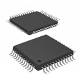
圖片僅供參考
K9F1G08U0D-SCB0
- 製造商
- 製造商。 部分 #K9F1G08U0D-SCB0
- 包
- 資料表
- 有現貨的5035
100%原創; 新
24小時準備發貨
365天保修
RFQ&; 獲得更多折扣
規格
| Manufacturer | Samsung Electro-Mechanics |
| Package | TSOPI-48 |
概述
Description
The K9F1G08U0D-SCB0 is a NAND flash memory chip produced by Samsung. It is designed for use in various applications, including mobile devices, consumer electronics, and embedded systems. This particular model features a 1 Gb (128 MB) capacity and utilizes a 3-bit-per-cell (TLC) architecture, allowing for increased storage density.
Key specifications include a standard NAND interface, with support for various programming and erasing cycles. It operates with a supply voltage typically around 2.7V to 3.6V, and it is optimized for high-speed data transfer and reliability. The chip incorporates error correction capabilities to ensure data integrity.
The K9F1G08U0D-SCB0 is suitable for applications requiring efficient storage solutions, making it a popular choice in the competitive landscape of flash memory technology. Its compact form factor and robust performance characteristics enable it to meet the demands of modern electronic devices.
Key specifications include a standard NAND interface, with support for various programming and erasing cycles. It operates with a supply voltage typically around 2.7V to 3.6V, and it is optimized for high-speed data transfer and reliability. The chip incorporates error correction capabilities to ensure data integrity.
The K9F1G08U0D-SCB0 is suitable for applications requiring efficient storage solutions, making it a popular choice in the competitive landscape of flash memory technology. Its compact form factor and robust performance characteristics enable it to meet the demands of modern electronic devices.
Features
The K9F1G08U0D-SCB0 is a NAND flash memory chip designed for high-density storage applications. Key features include:
1. Capacity: 1 Gb (Gigabit) of storage, suitable for various embedded systems.
2. Interface: It utilizes the NAND flash interface for efficient data transfer.
3. Architecture: Built on a multi-level cell (MLC) architecture, allowing for higher data storage density.
4. Data Transfer Rate: Offers fast read and write speeds, essential for performance-sensitive applications.
5. Endurance: Designed for a high number of program/erase cycles, enhancing longevity in applications.
6. Low Power Consumption: Optimized for low power usage, making it suitable for battery-operated devices.
7. Temperature Range: Operates within a wide temperature range, ensuring reliability in various environmental conditions.
8. Applications: Commonly used in consumer electronics, mobile devices, and other embedded applications.
Overall, the K9F1G08U0D-SCB0 is a reliable and efficient choice for modern storage needs.
1. Capacity: 1 Gb (Gigabit) of storage, suitable for various embedded systems.
2. Interface: It utilizes the NAND flash interface for efficient data transfer.
3. Architecture: Built on a multi-level cell (MLC) architecture, allowing for higher data storage density.
4. Data Transfer Rate: Offers fast read and write speeds, essential for performance-sensitive applications.
5. Endurance: Designed for a high number of program/erase cycles, enhancing longevity in applications.
6. Low Power Consumption: Optimized for low power usage, making it suitable for battery-operated devices.
7. Temperature Range: Operates within a wide temperature range, ensuring reliability in various environmental conditions.
8. Applications: Commonly used in consumer electronics, mobile devices, and other embedded applications.
Overall, the K9F1G08U0D-SCB0 is a reliable and efficient choice for modern storage needs.
Package
The K9F1G08U0D-SCB0 is a NAND Flash memory device packaged in a TSOP (Thin Small Outline Package). The TSOP package is designed for surface mounting, offering a compact footprint suitable for various electronic applications.
Pinout
The K9F1G08U0D-SCB0 is a NAND flash memory chip produced by Samsung. It has a total pin count of 48 pins.
The main functions of these pins include:
1. Data Pins (DQ0-DQ7): 8 data input/output pins for data transfer.
2. Command Pins (CLE, ALE): Command and address latch enable pins used to input commands and addresses.
3. Chip Enable (CE): Chip select pin to activate the memory chip.
4. Write Enable (WE): Used to initiate write operations.
5. Read Enable (RE): Used to initiate read operations.
6. Ready/Busy (R/B): Indicates the status of the chip (ready or busy).
7. Ground (VSS): Common ground connection.
8. Power Supply (VCC): Power supply pin.
9. Block Protection (BP0, BP1): Used for block protection features.
This chip is designed for high-density storage applications in consumer electronics and embedded systems.
The main functions of these pins include:
1. Data Pins (DQ0-DQ7): 8 data input/output pins for data transfer.
2. Command Pins (CLE, ALE): Command and address latch enable pins used to input commands and addresses.
3. Chip Enable (CE): Chip select pin to activate the memory chip.
4. Write Enable (WE): Used to initiate write operations.
5. Read Enable (RE): Used to initiate read operations.
6. Ready/Busy (R/B): Indicates the status of the chip (ready or busy).
7. Ground (VSS): Common ground connection.
8. Power Supply (VCC): Power supply pin.
9. Block Protection (BP0, BP1): Used for block protection features.
This chip is designed for high-density storage applications in consumer electronics and embedded systems.
Manufacturer
The K9F1G08U0D-SCB0 is a NAND flash memory chip manufactured by Samsung Electronics. Samsung is a South Korean multinational conglomerate known for its diverse range of products and services, including consumer electronics, semiconductors, telecommunications equipment, and more. The company is one of the world's largest producers of electronic components and is a leader in the semiconductor industry, particularly in memory technology. Samsung's semiconductor division specializes in manufacturing various types of memory chips, including DRAM and NAND flash, which are used in a wide array of devices such as smartphones, tablets, SSDs, and other electronics.
Application
The K9F1G08U0D-SCB0 is a NAND flash memory chip commonly used in various applications, including mobile devices, digital cameras, portable media players, and solid-state drives (SSDs). It serves as storage for data, applications, and firmware in consumer electronics, automotive systems, and industrial devices, providing high-density, non-volatile memory solutions for efficient data storage and retrieval.
Equivalent
The K9F1G08U0D-SCB0 is a 1 Gb NAND flash memory chip. Equivalent products include the Micron MT29F1G08ABAEAWP, Samsung K9F1G08U0D-PIB0, and Toshiba TC58NVG0S3HBAI4. Always check specific datasheets for compatibility regarding pin configuration, voltage, and timing parameters.
船舶
運輸管道我們
通過DHL、FedEx、TNT、UPS或您選擇的任何其他貨運代理提供全球運輸服務。
運費參攷(DHL/FedEx):
動態主要裝載: 運費從25美元到45美元(0.5公斤)不等,預計交貨時間為2-5個工作日。
聯邦快遞: 運費從25美元到40美元(0.5公斤)不等,預計交貨時間為3-7個工作日。
不斷電供應系統: 運費從25美元到45美元(0.5公斤)不等,預計交貨時間為3-7個工作日。
三硝基甲苯: 運費從25美元到65美元(0.5公斤)不等,預計交貨時間為3-7個工作日。
增强型短消息: 運費從30美元到50美元(0.5公斤)不等,預計交貨時間為7-15個工作日。
掛號: 運費為2-4美元(0.1公斤),預計交貨時間為5-20個工作日。
支付
Payment Methods
付款條件為100%預付。
現時,我們只接受以下付款方式:
1. 貝寶
2. 信用卡/借記卡
3. 電匯
類似的
-
![MX25R8035FM1IL0]() MX25R8035FM1IL0
Macronix
-
![MX25V1635FZNI]() MX25V1635FZNI
Macronix
-
![MX25V1635FZNQ03]() MX25V1635FZNQ03
Macronix
-
![MX66U1G45GXDI00]() MX66U1G45GXDI00
Macronix
-
![MX25V2033FM1I]() MX25V2033FM1I
Macronix
-
![MX25R6435FBDIL0]() MX25R6435FBDIL0
Macronix
-
![MX25L25673GMI-08G]() MX25L25673GMI-08G
Macronix
-
![MX25U51279GXDR00]() MX25U51279GXDR00
Macronix
-
![MX25U25643GZNI00]() MX25U25643GZNI00
Macronix
-
![MX25R1635FZUIH0]() MX25R1635FZUIH0
Macronix
-
![MX25U3232FZBI02]() MX25U3232FZBI02
Macronix
-
![MX25L6433FM2I-08G]() MX25L6433FM2I-08G
Macronix