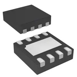
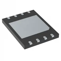
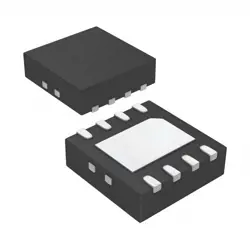
圖片僅供參考
IS25WP128F-JBLE
IC FLASH 128MBIT SPI/QUAD 8SOIC
- 製造商
- 製造商。 部分 #IS25WP128F-JBLE
- 包
- 資料表
- 有現貨的7144
100%原創; 新
24小時準備發貨
365天保修
RFQ&; 獲得更多折扣
規格
| Part Status | Active |
| DigiKey Programmable | Verified |
| Memory Type | Non-Volatile |
| Memory Format | FLASH |
| Technology | FLASH - NOR |
| Memory Size | 128Mbit |
| Memory Organization | 16M x 8 |
| Memory Interface | SPI - Quad I/O, QPI, DTR |
| Clock Frequency | 133 MHz |
| Write Cycle Time - Word, Page | 800µs |
| Voltage - Supply | 1.65V ~ 1.95V |
| Operating Temperature | -40°C ~ 105°C (TA) |
| Mounting Type | Surface Mount |
| Package / Case | 8-SOIC (0.209", 5.30mm Width) |
| Supplier Device Package | 8-SOIC |
| Base Product Number | IS25WP128 |
概述
Description
The IS25WP128F-JBLE is a serial NOR flash memory chip manufactured by ISSI (Integrated Silicon Solution, Inc.). It features a density of 128 megabits (16 megabytes) and operates on a voltage range of 2.7V to 3.6V. The device uses a quad-SPI (Serial Peripheral Interface) interface, which allows for faster data transfer rates compared to traditional SPI by enabling four data lines.
Key features include:
- High Read Speed: Supports up to 104 MHz clock frequency for high-performance applications.
- Low Power Consumption: Designed for low power operation, making it suitable for battery-powered devices.
- Flexible Erase and Program Options: Offers various block sizes for erasing and programming, enhancing versatility for different applications.
- Reliability: Endurance of up to 100,000 program/erase cycles and data retention up to 20 years.
This memory chip is commonly used in embedded systems, consumer electronics, and automotive applications, where reliable, high-speed memory storage is essential.
Features
The IS25WP128F-JBLE is a 128Mb (16MB) serial NOR flash memory device from ISSI. Key features include:
- Interface: Supports a Serial Peripheral Interface (SPI) with quad, dual, and single I/O modes for high-speed data transfer.
- Density: 128Mb capacity with x8 or x16 configurations available.
- Speed: Fast read speeds up to 104 MHz, enabling efficient data access.
- Operating Voltage: Operates between 2.7V and 3.6V, suitable for a variety of applications.
- Endurance: Offers a high endurance level with up to 100,000 program/erase cycles.
- Data Retention: Provides data retention of up to 20 years at 125°C.
- Flexible Architecture: Supports sector and block erase modes for efficient memory management.
- Packages: Available in various packages, including SOP, WSON, and BGA, for versatile integration into designs.
This device is commonly used in consumer electronics, automotive applications, and industrial settings for firmware storage and data logging.
Package
The IS25WP128F-JBLE is packaged in a WSON (Wettable Flank Quad Flat No-Lead) format, specifically a 8mm x 6mm, 24-pin configuration. This package type allows for a compact design and efficient thermal management, suitable for various applications in electronics.
Pinout
The IS25WP128F-JBLE is a serial NOR flash memory device with a total of 8 pins. It is designed for high-density applications and features a SPI (Serial Peripheral Interface) interface. Here’s a brief overview of its pin functions:
1. GND: Ground connection.
2. VCC: Power supply (typically 2.7V to 3.6V).
3. SCK: Serial Clock input for synchronizing communication.
4. CS#: Chip Select (active low) to enable the device.
5. MISO: Master In Slave Out, used for data output to the master.
6. MOSI: Master Out Slave In, used for data input from the master.
7. WP#: Write Protect (active low) to prevent writing to the memory.
8. HOLD#: Hold (active low) to pause communication without deactivating chip select.
This combination of pins allows the IS25WP128F-JBLE to function efficiently in embedded applications where non-volatile memory storage is required.
Manufacturer
The IS25WP128F-JBLE is manufactured by Integrated Silicon Solution, Inc. (ISSI). ISSI is a semiconductor company that specializes in designing and manufacturing integrated circuits (ICs) for various applications, including memory products like NOR Flash and SRAM, as well as analog products. Founded in 1988 and headquartered in San Jose, California, ISSI serves a diverse range of markets, including automotive, industrial, consumer electronics, and telecommunications. The company is known for its focus on high-performance, reliable memory solutions, and it aims to provide innovative products that meet the evolving needs of technology applications.
Application
The IS25WP128F-JBLE is a NOR Flash memory device commonly used in applications such as embedded systems, industrial automation, automotive electronics, consumer electronics, and telecommunications. It provides non-volatile storage for firmware, code execution, and data logging in devices like IoT gadgets, routers, and smart appliances due to its high density and reliability.
Equivalent
The IS25WP128F-JBLE chip is a 128Mb (16MB) NOR Flash memory device. Equivalent products include the Winbond W25Q128JV, Micron MT25QL128ABA, and Spansion S25FL128S. These chips offer similar functionality, capacities, and interfaces (SPI). Always verify specific requirements and features for compatibility.
船舶
運輸管道我們
通過DHL、FedEx、TNT、UPS或您選擇的任何其他貨運代理提供全球運輸服務。
運費參攷(DHL/FedEx):
動態主要裝載: 運費從25美元到45美元(0.5公斤)不等,預計交貨時間為2-5個工作日。
聯邦快遞: 運費從25美元到40美元(0.5公斤)不等,預計交貨時間為3-7個工作日。
不斷電供應系統: 運費從25美元到45美元(0.5公斤)不等,預計交貨時間為3-7個工作日。
三硝基甲苯: 運費從25美元到65美元(0.5公斤)不等,預計交貨時間為3-7個工作日。
增强型短消息: 運費從30美元到50美元(0.5公斤)不等,預計交貨時間為7-15個工作日。
掛號: 運費為2-4美元(0.1公斤),預計交貨時間為5-20個工作日。
支付
Payment Methods
付款條件為100%預付。
現時,我們只接受以下付款方式:
1. 貝寶
2. 信用卡/借記卡
3. 電匯
類似的
-
![MX25V5126FM1I]() MX25V5126FM1I
Macronix
-
![MX30LF2G28AD-TI]() MX30LF2G28AD-TI
Macronix
-
![MX25R6435FBDIL0]() MX25R6435FBDIL0
Macronix
-
![MX29GL512FHXFI-11G]() MX29GL512FHXFI-11..
Macronix
-
![MX25U25643GZNI00]() MX25U25643GZNI00
Macronix
-
![MX25L2006EM1I-12G]() MX25L2006EM1I-12G
Macronix
-
![MX25R1635FZUIH0]() MX25R1635FZUIH0
Macronix
-
![MX25L6433FM2I-08G]() MX25L6433FM2I-08G
Macronix
-
![MX25L12833FZ2I-10G]() MX25L12833FZ2I-10..
Macronix
-
![MX25L12833FZNI-10G]() MX25L12833FZNI-10..
Macronix
-
![MX29LV160DTTI-70G]() MX29LV160DTTI-70G
Macronix
-
![MX29F040CQI-70G]() MX29F040CQI-70G
Macronix