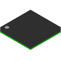
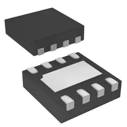
圖片僅供參考
HEF4015BT
Counter Shift Registers
- 製造商
- 製造商。 部分 #HEF4015BT
- 包
- 資料表
- 有現貨的16089
100%原創; 新
24小時準備發貨
365天保修
RFQ&; 獲得更多折扣
規格
概述
Description
HEF4015BT is a dual 4-bit static shift register integrated circuit. It is part of the HEF4000 series of CMOS logic devices and is commonly used in digital applications such as data storage, transfer, and processing. The chip can shift data either left or right, depending on the control inputs, allowing for flexible data manipulation.
Key features include a wide operating voltage range (typically 3V to 15V), low power consumption, and compatibility with various logic levels. The shift register operates in synchronous mode, meaning that data shifts occur on clock pulses, ensuring precise timing in digital circuits.
Applications include digital signal processing, temporary data storage, and interfacing between different digital components. The HEF4015BT is widely used in educational and hobbyist projects due to its ease of use and versatility.
Key features include a wide operating voltage range (typically 3V to 15V), low power consumption, and compatibility with various logic levels. The shift register operates in synchronous mode, meaning that data shifts occur on clock pulses, ensuring precise timing in digital circuits.
Applications include digital signal processing, temporary data storage, and interfacing between different digital components. The HEF4015BT is widely used in educational and hobbyist projects due to its ease of use and versatility.
Features
The HEF4015BT is a dual 4-bit static RAM integrated circuit (IC) that is part of the HEF4000 series of CMOS logic devices. Key features include:
1. Dual 4-bit Memory: Contains two independent 4-bit RAM blocks.
2. Low Power Consumption: Operates at low supply voltages, typically between 3V to 15V.
3. Asynchronous Read/Write: Allows direct data access without the need for clock signals.
4. High-Speed Operation: Capable of fast access times, suitable for various applications.
5. Tri-State Outputs: Provides tri-state outputs, enabling multiple ICs to share a common data bus without interference.
6. Wide Operating Temperature Range: Suitable for industrial applications, typically ranging from -40°C to +125°C.
7. DIP Package: Available in a Dual In-line Package (DIP), making it easy to integrate into circuits.
The HEF4015BT is ideal for use in digital memory applications, registers, and temporary data storage in various electronic systems.
1. Dual 4-bit Memory: Contains two independent 4-bit RAM blocks.
2. Low Power Consumption: Operates at low supply voltages, typically between 3V to 15V.
3. Asynchronous Read/Write: Allows direct data access without the need for clock signals.
4. High-Speed Operation: Capable of fast access times, suitable for various applications.
5. Tri-State Outputs: Provides tri-state outputs, enabling multiple ICs to share a common data bus without interference.
6. Wide Operating Temperature Range: Suitable for industrial applications, typically ranging from -40°C to +125°C.
7. DIP Package: Available in a Dual In-line Package (DIP), making it easy to integrate into circuits.
The HEF4015BT is ideal for use in digital memory applications, registers, and temporary data storage in various electronic systems.
Package
The HEF4015BT is typically packaged in a dual in-line package (DIP) format, specifically a 14-pin DIP. It may also be available in other package types, such as surface mount options, depending on the manufacturer.
Pinout
The HEF4015BT is a dual 4-bit static shift register. It features a total of 16 pins. The main functions of the pins are as follows:
1. Pins 1-2 (A, B): Data input for shift operations.
2. Pins 3-4 (Q1, Q2): Outputs for the first and second shift registers.
3. Pin 5 (S): Serial data input for shifting.
4. Pin 6 (R): Reset input to clear the registers.
5. Pin 7 (CLK): Clock input to control the shifting operation.
6. Pin 8 (GND): Ground connection.
7. Pins 9-10 (Q3, Q4): Outputs for the second shift register.
8. Pin 11 (VDD): Power supply connection.
9. Pins 12-15: These pins may include additional control inputs or outputs depending on the specific configuration of the device.
The HEF4015BT operates on a wide voltage range, and its functionality is utilized in various digital applications requiring data shifting and storage.
1. Pins 1-2 (A, B): Data input for shift operations.
2. Pins 3-4 (Q1, Q2): Outputs for the first and second shift registers.
3. Pin 5 (S): Serial data input for shifting.
4. Pin 6 (R): Reset input to clear the registers.
5. Pin 7 (CLK): Clock input to control the shifting operation.
6. Pin 8 (GND): Ground connection.
7. Pins 9-10 (Q3, Q4): Outputs for the second shift register.
8. Pin 11 (VDD): Power supply connection.
9. Pins 12-15: These pins may include additional control inputs or outputs depending on the specific configuration of the device.
The HEF4015BT operates on a wide voltage range, and its functionality is utilized in various digital applications requiring data shifting and storage.
Manufacturer
The HEF4015BT is manufactured by NXP Semiconductors, a company known for its expertise in the design and manufacturing of semiconductor devices. NXP specializes in various electronic components, including microcontrollers, processors, and analog chips, serving diverse markets such as automotive, industrial, and consumer electronics. The HEF4015BT specifically is a dual 4-stage static shift register, part of the 4000 series of CMOS logic ICs, which are widely used in digital circuits for tasks involving data storage and transfer. NXP Semiconductors is recognized for its innovation and plays a significant role in advancing technology in the semiconductor industry.
Application
The HEF4015BT is a dual 4-bit static RAM, commonly used in applications such as digital signal processing, temporary data storage, microcontroller interfacing, and buffering. It is suitable for use in memory expansion, data logging, and caching in embedded systems, as well as for implementing state machines and other logic functions in digital circuits.
Equivalent
The HEF4015BT is a dual 4-bit static shift register. Equivalent products include the 74HC595, 74HC164, and 74HC165, which offer similar functionalities in different configurations. The CD4015 and MC14515 are also alternatives, depending on specific application requirements and logic levels. Always check specifications for compatibility in voltage and performance.
船舶
運輸管道我們
通過DHL、FedEx、TNT、UPS或您選擇的任何其他貨運代理提供全球運輸服務。
運費參攷(DHL/FedEx):
動態主要裝載: 運費從25美元到45美元(0.5公斤)不等,預計交貨時間為2-5個工作日。
聯邦快遞: 運費從25美元到40美元(0.5公斤)不等,預計交貨時間為3-7個工作日。
不斷電供應系統: 運費從25美元到45美元(0.5公斤)不等,預計交貨時間為3-7個工作日。
三硝基甲苯: 運費從25美元到65美元(0.5公斤)不等,預計交貨時間為3-7個工作日。
增强型短消息: 運費從30美元到50美元(0.5公斤)不等,預計交貨時間為7-15個工作日。
掛號: 運費為2-4美元(0.1公斤),預計交貨時間為5-20個工作日。
支付
Payment Methods
付款條件為100%預付。
現時,我們只接受以下付款方式:
1. 貝寶
2. 信用卡/借記卡
3. 電匯
類似的
-
![MX25V1635FZNI]() MX25V1635FZNI
MX25V1635FZNI
Macronix
-
![MX25V1635FZNQ03]() MX25V1635FZNQ03
MX25V1635FZNQ03
Macronix
-
![MX25V5126FM1I]() MX25V5126FM1I
MX25V5126FM1I
Macronix
-
![MX25V2033FM1I]() MX25V2033FM1I
MX25V2033FM1I
Macronix
-
![MX25V16066M1I02]() MX25V16066M1I02
MX25V16066M1I02
Macronix
-
![MX25R3235FZNIL0]() MX25R3235FZNIL0
MX25R3235FZNIL0
Macronix
-
![MX25V16066M2I02]() MX25V16066M2I02
MX25V16066M2I02
Macronix
-
![MX25L8035EM2I-10G]() MX25L8035EM2I-10G
MX25L8035EM2I-10G
Macronix
-
![MX25R6435FBDIL0]() MX25R6435FBDIL0
MX25R6435FBDIL0
Macronix
-
![MX29GL512FHXFI-11G]() MX29GL512FHXFI-11..
MX29GL512FHXFI-11..
Macronix
-
![MX25U25643GZNI00]() MX25U25643GZNI00
MX25U25643GZNI00
Macronix
-
![MX25U3232FZBI02]() MX25U3232FZBI02
MX25U3232FZBI02
Macronix