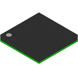
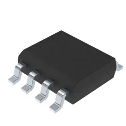
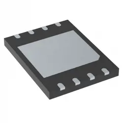
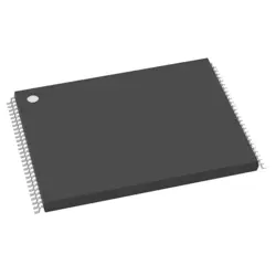
圖片僅供參考
GD25Q128EYIGR
IC FLASH 128MBIT SPI/QUAD 8WSON
- 製造商
- 製造商。 部分 #GD25Q128EYIGR
- 包
- 資料表
- 有現貨的5998
100%原創; 新
24小時準備發貨
365天保修
RFQ&; 獲得更多折扣
規格
| Part Status | Active |
| Memory Type | Non-Volatile |
| Memory Format | FLASH |
| Technology | FLASH - NOR (SLC) |
| Memory Size | 128Mbit |
| Memory Organization | 16M x 8 |
| Memory Interface | SPI - Quad I/O |
| Write Cycle Time - Word, Page | 70µs, 2.4ms |
| Voltage - Supply | 2.7V ~ 3.6V |
| Operating Temperature | -40°C ~ 85°C (TA) |
| Mounting Type | Surface Mount |
| Package / Case | 8-WDFN Exposed Pad |
| Supplier Device Package | 8-WSON (6x8) |
| Base Product Number | GD25Q128 |
| Clock Frequency | 133 MHz |
| Access Time | 7 ns |
概述
Description
The GD25Q128EYIGR is a 128 Mbit (16 MB) serial Flash memory chip, produced by GigaDevice. It is designed for high-performance applications and utilizes the standard Serial Peripheral Interface (SPI) for communication, which is widely used in embedded systems for its simplicity and efficiency. The chip offers a wide range of features, including high-speed read capabilities, low power consumption, and robust data retention and endurance.
Key features include a dual/quad SPI for faster data transfer rates, a deep power-down mode to conserve energy, and support for various security measures like block protection and secured OTP regions. The GD25Q128EYIGR operates over a wide temperature range, making it suitable for various applications, including consumer electronics, industrial automation, and automotive systems.
The device supports a voltage range typically between 2.7V to 3.6V and has an extended operating temperature range from -40°C to +85°C, ensuring reliability in diverse environmental conditions. Its compact packaging options, such as the 8-pin SOP and 8-contact WSON, facilitate easy integration into space-constrained designs. This memory chip is ideal for applications requiring reliable, high-capacity storage with the capability for frequent read and write operations.
Key features include a dual/quad SPI for faster data transfer rates, a deep power-down mode to conserve energy, and support for various security measures like block protection and secured OTP regions. The GD25Q128EYIGR operates over a wide temperature range, making it suitable for various applications, including consumer electronics, industrial automation, and automotive systems.
The device supports a voltage range typically between 2.7V to 3.6V and has an extended operating temperature range from -40°C to +85°C, ensuring reliability in diverse environmental conditions. Its compact packaging options, such as the 8-pin SOP and 8-contact WSON, facilitate easy integration into space-constrained designs. This memory chip is ideal for applications requiring reliable, high-capacity storage with the capability for frequent read and write operations.
Features
The GD25Q128EYIGR is a 128 Mbit (16 MB) serial flash memory chip produced by GigaDevice. Key features include:
1. Interface: It uses a Serial Peripheral Interface (SPI) supporting standard, dual, and quad SPI for versatile communication.
2. Performance: Offers fast read speeds up to 104 MHz in standard SPI mode and up to 133 MHz in dual/quad SPI modes, providing efficient data access.
3. Voltage: Operates within a wide voltage range of 2.7V to 3.6V, making it suitable for a variety of applications.
4. Erase/Program: Supports sector-wise erase (4KB), block erase (32KB or 64KB), and chip erase functions. Program operations are performed in pages of 256 bytes.
5. Endurance and Data Retention: Supports up to 100,000 program/erase cycles per sector and offers data retention of over 20 years.
6. Security: Features include a 64-bit unique identifier, block protection, and security registers for data protection.
7. Package Options: Available in multiple packages like SOP8, WSON8, and USON8, catering to different design requirements.
These attributes make the GD25Q128EYIGR suitable for various applications, such as consumer electronics, industrial devices, and automotive systems.
1. Interface: It uses a Serial Peripheral Interface (SPI) supporting standard, dual, and quad SPI for versatile communication.
2. Performance: Offers fast read speeds up to 104 MHz in standard SPI mode and up to 133 MHz in dual/quad SPI modes, providing efficient data access.
3. Voltage: Operates within a wide voltage range of 2.7V to 3.6V, making it suitable for a variety of applications.
4. Erase/Program: Supports sector-wise erase (4KB), block erase (32KB or 64KB), and chip erase functions. Program operations are performed in pages of 256 bytes.
5. Endurance and Data Retention: Supports up to 100,000 program/erase cycles per sector and offers data retention of over 20 years.
6. Security: Features include a 64-bit unique identifier, block protection, and security registers for data protection.
7. Package Options: Available in multiple packages like SOP8, WSON8, and USON8, catering to different design requirements.
These attributes make the GD25Q128EYIGR suitable for various applications, such as consumer electronics, industrial devices, and automotive systems.
Package
The GD25Q128EYIGR is a serial NOR Flash memory chip, and it typically comes in a WSON (Wafer-level Small Outline No-lead) package. This package type is designed for compact applications, allowing for reduced space on the PCB.
Pinout
The GD25Q128EYIGR is a serial NOR Flash memory chip produced by GigaDevice. It typically comes in an 8-pin package. Here's a brief overview of its pin configuration and functions:
1. CS# (Chip Select): Activates the device when low and enables communication.
2. DO/IO1 (Data Out/IO1): Serves as the data output during read operations and can also be used as an input/output in dual/quad I/O modes.
3. WP# (Write Protect): Used to protect the status register and memory content.
4. GND (Ground): Connects to the system ground.
5. DI/IO0 (Data In/IO0): Used for input data during write operations and as an I/O line in dual/quad modes.
6. CLK (Clock): Provides the clock signal for synchronizing data transfer.
7. RESET#/IO3: Resets the device or serves as an I/O line in quad mode.
8. VCC (Power Supply): Supplies the operating voltage to the chip.
This memory chip is commonly used for data storage in various applications, offering high-speed read/write operations and reliability.
1. CS# (Chip Select): Activates the device when low and enables communication.
2. DO/IO1 (Data Out/IO1): Serves as the data output during read operations and can also be used as an input/output in dual/quad I/O modes.
3. WP# (Write Protect): Used to protect the status register and memory content.
4. GND (Ground): Connects to the system ground.
5. DI/IO0 (Data In/IO0): Used for input data during write operations and as an I/O line in dual/quad modes.
6. CLK (Clock): Provides the clock signal for synchronizing data transfer.
7. RESET#/IO3: Resets the device or serves as an I/O line in quad mode.
8. VCC (Power Supply): Supplies the operating voltage to the chip.
This memory chip is commonly used for data storage in various applications, offering high-speed read/write operations and reliability.
Manufacturer
The GD25Q128EYIGR is manufactured by GigaDevice Semiconductor Inc. GigaDevice is a Chinese company specializing in the design and manufacture of semiconductor products. They are known for their flash memory, microcontrollers, and other related products. The company focuses on providing high-performance, cost-effective solutions for a wide range of applications, including consumer electronics, industrial systems, and automotive sectors.
Application
The GD25Q128EYIGR is a 128Mb serial flash memory chip commonly used in applications requiring reliable and high-speed data storage. Typical areas include consumer electronics, such as smart TVs and set-top boxes, computer peripherals, embedded systems, IoT devices, and automotive electronics. It supports execute-in-place (XIP) features, making it suitable for applications that demand fast boot times and real-time data processing.
Equivalent
The GD25Q128EYIGR is a 128Mb serial NOR Flash memory chip. Equivalent products with similar specifications include:
1. Winbond W25Q128JV
2. Macronix MX25L12835F
3. Micron MT25QL128
4. ISSI IS25LP128
5. Cypress/Spansion S25FL128S
These chips typically offer similar features such as SPI interface, comparable read/write speeds, and temperature ranges. Always check the datasheets for pin compatibility and specific feature matches.
1. Winbond W25Q128JV
2. Macronix MX25L12835F
3. Micron MT25QL128
4. ISSI IS25LP128
5. Cypress/Spansion S25FL128S
These chips typically offer similar features such as SPI interface, comparable read/write speeds, and temperature ranges. Always check the datasheets for pin compatibility and specific feature matches.
船舶
運輸管道我們
通過DHL、FedEx、TNT、UPS或您選擇的任何其他貨運代理提供全球運輸服務。
運費參攷(DHL/FedEx):
動態主要裝載: 運費從25美元到45美元(0.5公斤)不等,預計交貨時間為2-5個工作日。
聯邦快遞: 運費從25美元到40美元(0.5公斤)不等,預計交貨時間為3-7個工作日。
不斷電供應系統: 運費從25美元到45美元(0.5公斤)不等,預計交貨時間為3-7個工作日。
三硝基甲苯: 運費從25美元到65美元(0.5公斤)不等,預計交貨時間為3-7個工作日。
增强型短消息: 運費從30美元到50美元(0.5公斤)不等,預計交貨時間為7-15個工作日。
掛號: 運費為2-4美元(0.1公斤),預計交貨時間為5-20個工作日。
支付
Payment Methods
付款條件為100%預付。
現時,我們只接受以下付款方式:
1. 貝寶
2. 信用卡/借記卡
3. 電匯
類似的
-
![MX25L3233FZBI-08Q]() MX25L3233FZBI-08Q
MX25L3233FZBI-08Q
Macronix
-
![MX25V1635FZNI]() MX25V1635FZNI
MX25V1635FZNI
Macronix
-
![MX25V16066M1I02]() MX25V16066M1I02
MX25V16066M1I02
Macronix
-
![MX25R3235FZNIL0]() MX25R3235FZNIL0
MX25R3235FZNIL0
Macronix
-
![MX25V16066M2I02]() MX25V16066M2I02
MX25V16066M2I02
Macronix
-
![MX25R6435FBDIL0]() MX25R6435FBDIL0
MX25R6435FBDIL0
Macronix
-
![MX25L25673GMI-10G]() MX25L25673GMI-10G
MX25L25673GMI-10G
Macronix
-
![MX29GL512FHXFI-11G]() MX29GL512FHXFI-11..
MX29GL512FHXFI-11..
Macronix
-
![MX25L2006EM1I-12G]() MX25L2006EM1I-12G
MX25L2006EM1I-12G
Macronix
-
![MX25V1635FM2I]() MX25V1635FM2I
MX25V1635FM2I
Macronix
-
![MX25L12833FZ2I-10G]() MX25L12833FZ2I-10..
MX25L12833FZ2I-10..
Macronix
-
![MX29LV160DTTI-70G]() MX29LV160DTTI-70G
MX29LV160DTTI-70G
Macronix