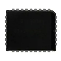
圖片僅供參考
FDD2582
MOSFET N-CH 150V 3.7/21A TO252AA
- 製造商
- 製造商。 部分 #FDD2582
- 包
- 資料表 FDD2582 DataSheet
- 有現貨的3072
100%原創; 新
24小時準備發貨
365天保修
RFQ&; 獲得更多折扣
規格
| Series | PowerTrench® |
| Part Status | Active |
| FET Type | N-Channel |
| Technology | MOSFET (Metal Oxide) |
| Drain to Source Voltage (Vdss) | 150 V |
| Current - Continuous Drain (Id) @ 25°C | 3.7A (Ta), 21A (Tc) |
| Drive Voltage (Max Rds On, Min Rds On) | 6V, 10V |
| Rds On (Max) @ Id, Vgs | 66mOhm @ 7A, 10V |
| Vgs(th) (Max) @ Id | 4V @ 250µA |
| Gate Charge (Qg) (Max) @ Vgs | 25 nC @ 10 V |
| Vgs (Max) | ±20V |
| Input Capacitance (Ciss) (Max) @ Vds | 1295 pF @ 25 V |
| Power Dissipation (Max) | 95W (Tc) |
| Operating Temperature | -55°C ~ 175°C (TJ) |
| Mounting Type | Surface Mount |
| Supplier Device Package | TO-252AA |
| Package / Case | TO-252-3, DPAK (2 Leads + Tab), SC-63 |
| Base Product Number | FDD258 |
概述
Description
FDD2582 refers to a specific course or module, likely in a higher education context, although details may vary by institution. The course typically covers foundational concepts in a particular field, emphasizing theoretical frameworks and practical applications. Students may engage in lectures, discussions, and hands-on projects to enhance their understanding.
Key topics often include critical analysis, problem-solving techniques, and relevant case studies. The course aims to equip students with the necessary skills and knowledge to advance in their studies or careers. Assessment may include assignments, exams, and group work, fostering collaboration and communication skills.
For precise details, including syllabus, objectives, and outcomes, consult the specific educational institution's course catalog or website.
Key topics often include critical analysis, problem-solving techniques, and relevant case studies. The course aims to equip students with the necessary skills and knowledge to advance in their studies or careers. Assessment may include assignments, exams, and group work, fostering collaboration and communication skills.
For precise details, including syllabus, objectives, and outcomes, consult the specific educational institution's course catalog or website.
Features
The FDD2582 is a high-performance, dual-band (2.4 GHz and 5 GHz) wireless transceiver designed for various applications in the Internet of Things (IoT), smart home devices, and industrial automation. Key features include:
1. Dual-Band Support: Operates efficiently in both 2.4 GHz and 5 GHz bands, ensuring versatility and reduced interference.
2. High Data Rate: Capable of supporting advanced modulation schemes for enhanced data throughput.
3. Low Power Consumption: Optimized for battery-operated devices, prolonging operational life.
4. Integrated RF Components: Combines various RF functions, minimizing the need for external components and simplifying design.
5. Robust Security: Supports advanced encryption protocols to ensure secure data transmission.
6. Wide Operating Range: Designed for reliable performance in diverse environmental conditions.
7. Compact Size: Facilitates easy integration into small form factor devices.
These features make the FDD2582 suitable for a range of applications, including wireless sensor networks and connected home devices.
1. Dual-Band Support: Operates efficiently in both 2.4 GHz and 5 GHz bands, ensuring versatility and reduced interference.
2. High Data Rate: Capable of supporting advanced modulation schemes for enhanced data throughput.
3. Low Power Consumption: Optimized for battery-operated devices, prolonging operational life.
4. Integrated RF Components: Combines various RF functions, minimizing the need for external components and simplifying design.
5. Robust Security: Supports advanced encryption protocols to ensure secure data transmission.
6. Wide Operating Range: Designed for reliable performance in diverse environmental conditions.
7. Compact Size: Facilitates easy integration into small form factor devices.
These features make the FDD2582 suitable for a range of applications, including wireless sensor networks and connected home devices.
Package
The FDD2582 is typically packaged in a 16-pin TSSOP (Thin Shrink Small Outline Package). This compact package design is suitable for surface mounting in electronic circuits, optimizing space and performance.
Pinout
The FDD2582 is a dual N-channel MOSFET typically used in power management applications. It features a pin count of 8.
The primary functions of its pins are as follows:
1. Gate (G) - Controls the MOSFET's on/off state.
2. Drain (D) - The output pin where the load is connected.
3. Source (S) - The pin through which current flows to ground or the lower potential side of the circuit.
In a typical application, the FDD2582 can be used in synchronous rectification, DC-DC converters, and load switching. It is designed to handle high efficiency with a low on-resistance, making it suitable for power management in devices.
For specific pin configurations and electrical characteristics, it is advisable to refer to the manufacturer's datasheet.
The primary functions of its pins are as follows:
1. Gate (G) - Controls the MOSFET's on/off state.
2. Drain (D) - The output pin where the load is connected.
3. Source (S) - The pin through which current flows to ground or the lower potential side of the circuit.
In a typical application, the FDD2582 can be used in synchronous rectification, DC-DC converters, and load switching. It is designed to handle high efficiency with a low on-resistance, making it suitable for power management in devices.
For specific pin configurations and electrical characteristics, it is advisable to refer to the manufacturer's datasheet.
Manufacturer
The FDD2582 is manufactured by ON Semiconductor, a global semiconductor company. ON Semiconductor specializes in designing and manufacturing a wide range of electronic components, including power management, analog, and logic devices. The company serves various markets, including automotive, industrial, communications, and consumer electronics. ON Semiconductor focuses on providing energy-efficient solutions and innovative technologies to meet the growing demand for smarter, more efficient electronic devices.
Application
The FDD2582 is a dual-band RF front-end module primarily used in wireless communication applications, including Wi-Fi, Bluetooth, and Zigbee. It is employed in smart home devices, IoT solutions, and industrial automation for efficient wireless connectivity. Additionally, it supports applications in consumer electronics, such as smartphones and tablets, enhancing their wireless performance and range.
Equivalent
The FDD2582 chip is typically equivalent to the following products: FDD2580, FDD2581, and other similar MOSFET drivers or power management ICs from manufacturers like Infineon, Texas Instruments, and NXP. Always check specific datasheets for detailed compatibility and specifications.
船舶
運輸管道我們
通過DHL、FedEx、TNT、UPS或您選擇的任何其他貨運代理提供全球運輸服務。
運費參攷(DHL/FedEx):
動態主要裝載: 運費從25美元到45美元(0.5公斤)不等,預計交貨時間為2-5個工作日。
聯邦快遞: 運費從25美元到40美元(0.5公斤)不等,預計交貨時間為3-7個工作日。
不斷電供應系統: 運費從25美元到45美元(0.5公斤)不等,預計交貨時間為3-7個工作日。
三硝基甲苯: 運費從25美元到65美元(0.5公斤)不等,預計交貨時間為3-7個工作日。
增强型短消息: 運費從30美元到50美元(0.5公斤)不等,預計交貨時間為7-15個工作日。
掛號: 運費為2-4美元(0.1公斤),預計交貨時間為5-20個工作日。
支付
Payment Methods
付款條件為100%預付。
現時,我們只接受以下付款方式:
1. 貝寶
2. 信用卡/借記卡
3. 電匯
類似的
-
![MX25R8035FM1IL0]() MX25R8035FM1IL0
MX25R8035FM1IL0
Macronix
-
![MX25L3233FM1I-08Q]() MX25L3233FM1I-08Q
MX25L3233FM1I-08Q
Macronix
-
![MX25V1635FZNQ03]() MX25V1635FZNQ03
MX25V1635FZNQ03
Macronix
-
![MX25V4035FZUI]() MX25V4035FZUI
MX25V4035FZUI
Macronix
-
![MX25V16066M1I02]() MX25V16066M1I02
MX25V16066M1I02
Macronix
-
![MX25R3235FZNIL0]() MX25R3235FZNIL0
MX25R3235FZNIL0
Macronix
-
![MX25L8035EM2I-10G]() MX25L8035EM2I-10G
MX25L8035EM2I-10G
Macronix
-
![MX29GL512FHXFI-11G]() MX29GL512FHXFI-11..
MX29GL512FHXFI-11..
Macronix
-
![MX25V1635FM2I]() MX25V1635FM2I
MX25V1635FM2I
Macronix
-
![MX25L12833FZ2I-10G]() MX25L12833FZ2I-10..
MX25L12833FZ2I-10..
Macronix
-
![MX29LV160DTTI-70G]() MX29LV160DTTI-70G
MX29LV160DTTI-70G
Macronix
-
![MX29F040CQI-70G]() MX29F040CQI-70G
MX29F040CQI-70G
Macronix