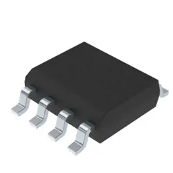
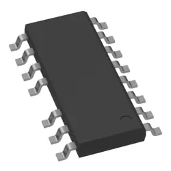
圖片僅供參考
FDC5612
MOSFET N-CH 60V 4.3A SUPERSOT6
- 製造商
- 製造商。 部分 #FDC5612
- 包 SSOT-6
- 資料表
- 有現貨的6813
100%原創; 新
24小時準備發貨
365天保修
RFQ&; 獲得更多折扣
規格
| Package | Tape & Reel (TR),Cut Tape (CT) |
| Series | PowerTrench® |
| ProductStatus | Active |
| FETType | N-Channel |
| Technology | MOSFET (Metal Oxide) |
| DraintoSourceVoltage(Vdss) | 60 V |
| Current-ContinuousDrain(Id)@25°C | 4.3A (Ta) |
| DriveVoltage(MaxRdsOnMinRdsOn) | 6V, 10V |
| RdsOn(Max)@IdVgs | 55mOhm @ 4.3A, 10V |
| Vgs(th)(Max)@Id | 4V @ 250µA |
| GateCharge(Qg)(Max)@Vgs | 18 nC @ 10 V |
| Vgs(Max) | ±20V |
| InputCapacitance(Ciss)(Max)@Vds | 650 pF @ 25 V |
| PowerDissipation(Max) | 1.6W (Ta) |
| OperatingTemperature | -55°C ~ 150°C (TJ) |
| MountingType | Surface Mount |
| SupplierDevicePackage | SuperSOT™-6 |
概述
Description
FDC5612 is a specialized integrated circuit designed primarily for use in power management applications. It is a part of the family of devices that excel in controlling and regulating power supplies, particularly in battery-operated systems. The FDC5612 features a high-efficiency buck converter for stepping down voltage with minimal loss, making it suitable for mobile and portable devices.
Key features include a wide input voltage range, low quiescent current, and various protection mechanisms, such as overcurrent and thermal shutdown. Its advanced control architecture allows for stable operation across varying loads and input conditions. The chip is often used in applications like smartphones, tablets, and IoT devices, where energy efficiency is paramount.
The FDC5612 also supports various external components for configuring output voltage and current, enhancing its versatility. Overall, it provides a compact and efficient solution for designers looking to optimize power delivery in modern electronic devices.
Key features include a wide input voltage range, low quiescent current, and various protection mechanisms, such as overcurrent and thermal shutdown. Its advanced control architecture allows for stable operation across varying loads and input conditions. The chip is often used in applications like smartphones, tablets, and IoT devices, where energy efficiency is paramount.
The FDC5612 also supports various external components for configuring output voltage and current, enhancing its versatility. Overall, it provides a compact and efficient solution for designers looking to optimize power delivery in modern electronic devices.
Features
The FDC5612 is a high-performance, low-power dual-channel analog-to-digital converter (ADC) designed for various applications, including industrial automation, medical devices, and consumer electronics. Key features include:
1. Resolution: 12-bit resolution provides accurate digital representation of analog signals.
2. Sampling Rate: Capable of high sample rates, enabling fast data acquisition.
3. Input Range: Supports various input voltage ranges, enhancing versatility.
4. Low Power Consumption: Optimized for battery-operated devices, ensuring efficient operation.
5. Integrated Reference: On-chip voltage reference simplifies circuit design.
6. Differential Input: Allows for improved noise rejection and better signal integrity.
7. SPI Interface: Facilitates easy communication with microcontrollers and other digital systems.
8. Temperature Range: Operates over a wide temperature range, suitable for harsh environments.
9. Small Form Factor: Compact package design allows for space-saving in PCB layouts.
These features make the FDC5612 suitable for precise and efficient data acquisition in various electronic applications.
1. Resolution: 12-bit resolution provides accurate digital representation of analog signals.
2. Sampling Rate: Capable of high sample rates, enabling fast data acquisition.
3. Input Range: Supports various input voltage ranges, enhancing versatility.
4. Low Power Consumption: Optimized for battery-operated devices, ensuring efficient operation.
5. Integrated Reference: On-chip voltage reference simplifies circuit design.
6. Differential Input: Allows for improved noise rejection and better signal integrity.
7. SPI Interface: Facilitates easy communication with microcontrollers and other digital systems.
8. Temperature Range: Operates over a wide temperature range, suitable for harsh environments.
9. Small Form Factor: Compact package design allows for space-saving in PCB layouts.
These features make the FDC5612 suitable for precise and efficient data acquisition in various electronic applications.
Package
The FDC5612 is typically available in a 28-pin TSSOP (Thin Shrink Small Outline Package) format. This compact package design allows for efficient space utilization on printed circuit boards while maintaining performance in electronic applications.
Pinout
The FDC5612 is a dual-channel, high-speed, 12-bit analog-to-digital converter (ADC) with a pin count of 28 pins. Its primary functions include converting analog signals into digital data, suitable for various applications such as instrumentation, data acquisition, and signal processing.
Key features include:
- Dual-channel operation for simultaneous sampling.
- 12-bit resolution providing high accuracy.
- Serial interface (SPI) for data communication.
- Sample rates up to 1 Msps.
Typical pins include:
- Power supply pins (VDD, VSS)
- Analog input pins (AIN1, AIN2)
- Digital output pins (DOUT)
- Control pins (CS, SCLK, DIN)
The FDC5612 is designed for efficient performance in embedded systems requiring precise digital representations of analog signals.
Key features include:
- Dual-channel operation for simultaneous sampling.
- 12-bit resolution providing high accuracy.
- Serial interface (SPI) for data communication.
- Sample rates up to 1 Msps.
Typical pins include:
- Power supply pins (VDD, VSS)
- Analog input pins (AIN1, AIN2)
- Digital output pins (DOUT)
- Control pins (CS, SCLK, DIN)
The FDC5612 is designed for efficient performance in embedded systems requiring precise digital representations of analog signals.
Manufacturer
The FDC5612 is manufactured by Fairchild Semiconductor, which is now part of ON Semiconductor. Fairchild Semiconductor was known for its semiconductor solutions, including power management, analog, and interface products. The company played a significant role in the development of the semiconductor industry and specialized in providing a wide range of electronic components for various applications, including automotive, industrial, and consumer electronics. Today, as ON Semiconductor, it continues to focus on sustainable energy solutions and advanced technologies in the semiconductor sector.
Application
The FDC5612 is a high-precision capacitive sensing IC used primarily in applications such as proximity sensing, touch sensing, level sensing, and industrial automation. It is ideal for liquid level measurement, fluid detection, and non-contact sensing applications in consumer electronics, automotive systems, and home appliances. Its ability to accurately measure capacitance makes it useful in various sensing applications where precise detection and measurement are required.
Equivalent
The FDC5612 chip is a dual-channel, high-speed comparator. Equivalent products include the LM393, TLV3702, and MCP6541, which also provide dual comparator functionality. Additional alternatives might include the MAX9014 and LTC6752, depending on specific application requirements such as speed and voltage range. Always verify specs for compatibility with your design.
船舶
運輸管道我們
通過DHL、FedEx、TNT、UPS或您選擇的任何其他貨運代理提供全球運輸服務。
運費參攷(DHL/FedEx):
動態主要裝載: 運費從25美元到45美元(0.5公斤)不等,預計交貨時間為2-5個工作日。
聯邦快遞: 運費從25美元到40美元(0.5公斤)不等,預計交貨時間為3-7個工作日。
不斷電供應系統: 運費從25美元到45美元(0.5公斤)不等,預計交貨時間為3-7個工作日。
三硝基甲苯: 運費從25美元到65美元(0.5公斤)不等,預計交貨時間為3-7個工作日。
增强型短消息: 運費從30美元到50美元(0.5公斤)不等,預計交貨時間為7-15個工作日。
掛號: 運費為2-4美元(0.1公斤),預計交貨時間為5-20個工作日。
支付
Payment Methods
付款條件為100%預付。
現時,我們只接受以下付款方式:
1. 貝寶
2. 信用卡/借記卡
3. 電匯
類似的
-
![MX25L3233FZBI-08Q]() MX25L3233FZBI-08Q
MX25L3233FZBI-08Q
Macronix
-
![MX29F400CBTI-70G]() MX29F400CBTI-70G
MX29F400CBTI-70G
Macronix
-
![MX25V5126FM1I]() MX25V5126FM1I
MX25V5126FM1I
Macronix
-
![MX25R3235FZNIL0]() MX25R3235FZNIL0
MX25R3235FZNIL0
Macronix
-
![MX25L25673GMI-08G]() MX25L25673GMI-08G
MX25L25673GMI-08G
Macronix
-
![MX29GL512FHXFI-11G]() MX29GL512FHXFI-11..
MX29GL512FHXFI-11..
Macronix
-
![MX25U25643GZNI00]() MX25U25643GZNI00
MX25U25643GZNI00
Macronix
-
![MX25V1635FM2I]() MX25V1635FM2I
MX25V1635FM2I
Macronix
-
![MX29LV160DTTI-70G]() MX29LV160DTTI-70G
MX29LV160DTTI-70G
Macronix
-
![MX29F040CTI-70G]() MX29F040CTI-70G
MX29F040CTI-70G
Macronix
-
![MX25L25735FMI-10G]() MX25L25735FMI-10G
MX25L25735FMI-10G
Macronix
-
![MX25L1006EMI-10G]() MX25L1006EMI-10G
MX25L1006EMI-10G
Macronix