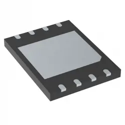
圖片僅供參考
EP4CE10F17I7N
IC FPGA 179 I/O 256FBGA
- 製造商
- 製造商。 部分 #EP4CE10F17I7N
- 包 FBGA-256
- 資料表
- 有現貨的3614
100%原創; 新
24小時準備發貨
365天保修
RFQ&; 獲得更多折扣
規格
| Package | Tray |
| Series | Cyclone® IV E |
| ProductStatus | Active |
| NumberofLABs/CLBs | 645 |
| NumberofLogicElements/Cells | 10320 |
| TotalRAMBits | 423936 |
| NumberofI/O | 179 |
| Voltage-Supply | 1.15V ~ 1.25V |
| MountingType | Surface Mount |
| OperatingTemperature | -40°C ~ 100°C (TJ) |
| Package/Case | 256-LBGA |
概述
Description
The EP4CE10F17I7N is a specific model of FPGA (Field Programmable Gate Array) from Intel's Cyclone IV family. It features a maximum of 10,000 logic elements, making it suitable for a range of applications including digital signal processing, embedded systems, and custom computing solutions. The "F17" in its designation indicates a specific package size and pin count, while "I7" refers to the industrial temperature grade, ensuring reliable operation in a wider temperature range. The "N" at the end signifies it is a lead-free, RoHS-compliant product.
This FPGA supports multiple I/O standards and offers integrated DSP blocks, memory interfaces, and a flexible architecture that allows for extensive customization. The EP4CE10F17I7N is ideal for applications demanding low power consumption combined with moderate performance, making it a popular choice for designers looking to create efficient, high-performance designs in a compact format.
This FPGA supports multiple I/O standards and offers integrated DSP blocks, memory interfaces, and a flexible architecture that allows for extensive customization. The EP4CE10F17I7N is ideal for applications demanding low power consumption combined with moderate performance, making it a popular choice for designers looking to create efficient, high-performance designs in a compact format.
Features
The EP4CE10F17I7N is a member of the Altera Cyclone IV FPGA family. Key features include:
1. Logic Elements: It contains approximately 10,000 logic elements (LEs) for implementing complex logic functions.
2. Memory: Supports on-chip memory with up to 240 Kbits of RAM, allowing for efficient data handling.
3. I/O Pins: Offers 17 dedicated I/O pins, supporting various I/O standards such as LVTTL, LVCMOS, and PCI.
4. Power Efficiency: Designed for low power consumption, making it suitable for portable and battery-operated applications.
5. Performance: Operates at a maximum clock frequency of approximately 150 MHz, providing flexibility for a range of applications.
6. Development Support: Compatible with the Quartus Prime development software, enabling easy design implementation and debugging.
These features make the EP4CE10F17I7N suitable for applications in communications, industrial control, and consumer electronics.
1. Logic Elements: It contains approximately 10,000 logic elements (LEs) for implementing complex logic functions.
2. Memory: Supports on-chip memory with up to 240 Kbits of RAM, allowing for efficient data handling.
3. I/O Pins: Offers 17 dedicated I/O pins, supporting various I/O standards such as LVTTL, LVCMOS, and PCI.
4. Power Efficiency: Designed for low power consumption, making it suitable for portable and battery-operated applications.
5. Performance: Operates at a maximum clock frequency of approximately 150 MHz, providing flexibility for a range of applications.
6. Development Support: Compatible with the Quartus Prime development software, enabling easy design implementation and debugging.
These features make the EP4CE10F17I7N suitable for applications in communications, industrial control, and consumer electronics.
Package
The EP4CE10F17I7N is packaged in a 144-pin Fine Pitch Ball Grid Array (FPBGA) format.
Pinout
The EP4CE10F17I7N is a model from the Intel (formerly Altera) Cyclone IV series of FPGAs. It has a total pin count of 144 pins.
The primary functions of these pins include:
1. I/O Pins: Configurable for various input/output operations, enabling communication with external devices.
2. Power Pins: Supply voltage and ground connections necessary for FPGA operation.
3. Clock Pins: Dedicated pins for clock signals, essential for synchronizing operations within the FPGA.
4. Configuration Pins: Used for programming and configuring the FPGA upon power-up.
5. JTAG Pins: For boundary scan and in-system programming.
The EP4CE10F17I7N is designed for applications requiring a balance of performance and cost-effectiveness, suitable for consumer electronics, automotive, and industrial control systems.
The primary functions of these pins include:
1. I/O Pins: Configurable for various input/output operations, enabling communication with external devices.
2. Power Pins: Supply voltage and ground connections necessary for FPGA operation.
3. Clock Pins: Dedicated pins for clock signals, essential for synchronizing operations within the FPGA.
4. Configuration Pins: Used for programming and configuring the FPGA upon power-up.
5. JTAG Pins: For boundary scan and in-system programming.
The EP4CE10F17I7N is designed for applications requiring a balance of performance and cost-effectiveness, suitable for consumer electronics, automotive, and industrial control systems.
Manufacturer
The EP4CE10F17I7N is manufactured by Intel Corporation, specifically under its Programmable Solutions Group, which was formerly known as Altera prior to Intel's acquisition in 2015. Intel is a multinational technology company primarily known for designing and manufacturing microprocessors and semiconductor products. The company specializes in various sectors, including computing, data centers, and artificial intelligence. Its programmable logic devices, like the EP4CE10F17I7N, are used in a range of applications including telecommunications, automotive, industrial, and consumer electronics, providing flexibility for hardware design through field-programmable gate arrays (FPGAs).
Application
The EP4CE10F17I7N is a Cyclone IV FPGA from Intel (formerly Altera) designed for various applications, including digital signal processing, telecommunications, industrial automation, automotive systems, and consumer electronics. Its low power consumption and adaptability make it suitable for embedded systems, data processing, and real-time control applications. Additionally, it is utilized in prototyping and educational settings for developing custom hardware solutions.
Equivalent
The EP4CE10F17I7N is an Altera (Intel) Cyclone IV FPGA. Equivalent products include:
1. Lattice ECP3-70 - Similar low-cost, low-power FPGA.
2. Xilinx Spartan-6 XC6SLX9 - Comparable in performance and resources.
3. Microsemi SmartFusion2 M2S010 - Offers integrated ARM Cortex-M3 with FPGA.
Always check specifications and compatibility for your specific application.
1. Lattice ECP3-70 - Similar low-cost, low-power FPGA.
2. Xilinx Spartan-6 XC6SLX9 - Comparable in performance and resources.
3. Microsemi SmartFusion2 M2S010 - Offers integrated ARM Cortex-M3 with FPGA.
Always check specifications and compatibility for your specific application.
船舶
運輸管道我們
通過DHL、FedEx、TNT、UPS或您選擇的任何其他貨運代理提供全球運輸服務。
運費參攷(DHL/FedEx):
動態主要裝載: 運費從25美元到45美元(0.5公斤)不等,預計交貨時間為2-5個工作日。
聯邦快遞: 運費從25美元到40美元(0.5公斤)不等,預計交貨時間為3-7個工作日。
不斷電供應系統: 運費從25美元到45美元(0.5公斤)不等,預計交貨時間為3-7個工作日。
三硝基甲苯: 運費從25美元到65美元(0.5公斤)不等,預計交貨時間為3-7個工作日。
增强型短消息: 運費從30美元到50美元(0.5公斤)不等,預計交貨時間為7-15個工作日。
掛號: 運費為2-4美元(0.1公斤),預計交貨時間為5-20個工作日。
支付
Payment Methods
付款條件為100%預付。
現時,我們只接受以下付款方式:
1. 貝寶
2. 信用卡/借記卡
3. 電匯
類似的
-
![MX25R8035FM1IL0]() MX25R8035FM1IL0
Macronix
-
![MX66U1G45GXDI00]() MX66U1G45GXDI00
Macronix
-
![MX25V5126FM1I]() MX25V5126FM1I
Macronix
-
![MX25V4035FZUI]() MX25V4035FZUI
Macronix
-
![MX25V16066M1I02]() MX25V16066M1I02
Macronix
-
![MX30LF2G28AD-TI]() MX30LF2G28AD-TI
Macronix
-
![MX29GL512FHXFI-11G]() MX29GL512FHXFI-11..
Macronix
-
![MX25R1635FZUIH0]() MX25R1635FZUIH0
Macronix
-
![MX25V1635FM2I]() MX25V1635FM2I
Macronix
-
![MX25L6433FM2I-08G]() MX25L6433FM2I-08G
Macronix
-
![MX25L12833FM2I-10G]() MX25L12833FM2I-10..
Macronix
-
![MX25L12833FZ2I-10G]() MX25L12833FZ2I-10..
Macronix