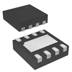
圖片僅供參考
EP2C5T144C8N
IC FPGA 89 I/O 144TQFP
- 製造商
- 製造商。 部分 #EP2C5T144C8N
- 包 TQFP-144
- 資料表
- 有現貨的7817
100%原創; 新
24小時準備發貨
365天保修
RFQ&; 獲得更多折扣
規格
| Package | Tray |
| Series | Cyclone® II |
| ProductStatus | Active |
| NumberofLABs/CLBs | 288 |
| NumberofLogicElements/Cells | 4608 |
| TotalRAMBits | 119808 |
| NumberofI/O | 89 |
| Voltage-Supply | 1.15V ~ 1.25V |
| MountingType | Surface Mount |
| OperatingTemperature | 0°C ~ 85°C (TJ) |
| Package/Case | 144-LQFP |
概述
Description
The EP2C5T144C8N is a member of the Cyclone II series of FPGAs (Field Programmable Gate Arrays) from Intel (formerly Altera). It features 2,304 logic elements (LEs), 144 I/O pins, and operates with a maximum clock frequency of up to 100 MHz. The device is built on a 90nm process technology and offers a range of features suitable for various applications, including digital signal processing, communication systems, and embedded control.
Key specifications include:
- Logic Element Count: 2,304 LEs
- Memory: Up to 128 Kbits of embedded memory
- I/O Standards: Supports various I/O standards like LVCMOS and LVTTL.
- Power Consumption: Low power operation, making it suitable for portable applications.
The EP2C5T144C8N is often used in educational and prototype applications due to its versatility, ease of use, and comprehensive development support through Intel's Quartus Prime software, which provides tools for design entry, synthesis, and programming.
Key specifications include:
- Logic Element Count: 2,304 LEs
- Memory: Up to 128 Kbits of embedded memory
- I/O Standards: Supports various I/O standards like LVCMOS and LVTTL.
- Power Consumption: Low power operation, making it suitable for portable applications.
The EP2C5T144C8N is often used in educational and prototype applications due to its versatility, ease of use, and comprehensive development support through Intel's Quartus Prime software, which provides tools for design entry, synthesis, and programming.
Features
The EP2C5T144C8N is a Cyclone II series FPGA from Intel (formerly Altera), featuring a 5,000 logic element (LE) architecture. Key specifications include:
- Logic Elements: 5,000 LE with 2-input look-up tables (LUTs) and flip-flops.
- Memory: 192 Kbits of embedded memory.
- I/O Pins: 144 available pins, supporting various I/O standards.
- Operating Voltage: Typically operates at 1.2V core voltage.
- Speed Grade: C8 speed grade, allowing for moderate performance.
- Power Consumption: Low power consumption, making it suitable for portable applications.
- Development Tools: Compatible with Quartus Prime software for design and simulation.
- Applications: Ideal for applications in communications, automotive, industrial control, and consumer electronics due to its balance of performance and power efficiency.
This FPGA is suitable for entry-level designs requiring moderate logic capacity and flexibility.
- Logic Elements: 5,000 LE with 2-input look-up tables (LUTs) and flip-flops.
- Memory: 192 Kbits of embedded memory.
- I/O Pins: 144 available pins, supporting various I/O standards.
- Operating Voltage: Typically operates at 1.2V core voltage.
- Speed Grade: C8 speed grade, allowing for moderate performance.
- Power Consumption: Low power consumption, making it suitable for portable applications.
- Development Tools: Compatible with Quartus Prime software for design and simulation.
- Applications: Ideal for applications in communications, automotive, industrial control, and consumer electronics due to its balance of performance and power efficiency.
This FPGA is suitable for entry-level designs requiring moderate logic capacity and flexibility.
Package
The EP2C5T144C8N is packaged in a TQFP (Thin Quad Flat Package) type with 144 pins.
Pinout
The EP2C5T144C8N is a field-programmable gate array (FPGA) from Intel's Cyclone II family. It features a total of 144 pins.
The primary functions of these pins include:
1. I/O Pins: Used for general input/output operations, allowing the FPGA to interface with external components.
2. Power Pins: Provide necessary power supply connections, including VCC and ground (GND).
3. Clock Pins: Support clock inputs for timing control and synchronization of operations within the FPGA.
4. Configuration Pins: Used for programming and configuring the FPGA at startup.
5. JTAG Pins: Facilitate debugging and programming through the Joint Test Action Group (JTAG) interface.
The EP2C5T144C8N is suitable for a variety of applications, including digital signal processing, embedded systems, and custom logic design, with its pin configuration enabling flexibility in circuit design.
The primary functions of these pins include:
1. I/O Pins: Used for general input/output operations, allowing the FPGA to interface with external components.
2. Power Pins: Provide necessary power supply connections, including VCC and ground (GND).
3. Clock Pins: Support clock inputs for timing control and synchronization of operations within the FPGA.
4. Configuration Pins: Used for programming and configuring the FPGA at startup.
5. JTAG Pins: Facilitate debugging and programming through the Joint Test Action Group (JTAG) interface.
The EP2C5T144C8N is suitable for a variety of applications, including digital signal processing, embedded systems, and custom logic design, with its pin configuration enabling flexibility in circuit design.
Manufacturer
The EP2C5T144C8N is manufactured by Intel Corporation, specifically under its Altera product line, which focuses on field-programmable gate arrays (FPGAs). Intel is a multinational corporation known primarily for its semiconductor products, including microprocessors and various computing technologies. The company designs and manufactures a wide range of electronic components and systems, serving industries such as computing, data centers, networking, and the Internet of Things (IoT). Established in 1968, Intel has evolved to become a leader in the technology sector, focusing on innovation and development to meet the growing demands of the digital world.
Application
The EP2C5T144C8N is a Cyclone II FPGA from Intel (formerly Altera) used in various applications such as digital signal processing, embedded systems, video and image processing, communications, industrial automation, and control systems. Its flexibility and programmable logic make it suitable for prototyping, custom hardware acceleration, and implementing complex algorithms in real-time applications.
Equivalent
The EP2C5T144C8N is an Altera Cyclone II FPGA. Equivalent products include the Lattice MachXO2, Xilinx Spartan-6, and Microsemi SmartFusion2 series FPGAs. Always check specific requirements such as I/O count, logic cells, and performance to ensure compatibility.
船舶
運輸管道我們
通過DHL、FedEx、TNT、UPS或您選擇的任何其他貨運代理提供全球運輸服務。
運費參攷(DHL/FedEx):
動態主要裝載: 運費從25美元到45美元(0.5公斤)不等,預計交貨時間為2-5個工作日。
聯邦快遞: 運費從25美元到40美元(0.5公斤)不等,預計交貨時間為3-7個工作日。
不斷電供應系統: 運費從25美元到45美元(0.5公斤)不等,預計交貨時間為3-7個工作日。
三硝基甲苯: 運費從25美元到65美元(0.5公斤)不等,預計交貨時間為3-7個工作日。
增强型短消息: 運費從30美元到50美元(0.5公斤)不等,預計交貨時間為7-15個工作日。
掛號: 運費為2-4美元(0.1公斤),預計交貨時間為5-20個工作日。
支付
Payment Methods
付款條件為100%預付。
現時,我們只接受以下付款方式:
1. 貝寶
2. 信用卡/借記卡
3. 電匯
類似的
-
![MX25V1635FZNI]() MX25V1635FZNI
MX25V1635FZNI
Macronix
-
![MX25V4035FZUI]() MX25V4035FZUI
MX25V4035FZUI
Macronix
-
![MX25V16066M1I02]() MX25V16066M1I02
MX25V16066M1I02
Macronix
-
![MX25V16066M2I02]() MX25V16066M2I02
MX25V16066M2I02
Macronix
-
![MX30LF2G28AD-TI]() MX30LF2G28AD-TI
MX30LF2G28AD-TI
Macronix
-
![MX25L8035EM2I-10G]() MX25L8035EM2I-10G
MX25L8035EM2I-10G
Macronix
-
![MX25R6435FBDIL0]() MX25R6435FBDIL0
MX25R6435FBDIL0
Macronix
-
![MX25L25673GMI-10G]() MX25L25673GMI-10G
MX25L25673GMI-10G
Macronix
-
![MX25U51279GXDR00]() MX25U51279GXDR00
MX25U51279GXDR00
Macronix
-
![MX25U25643GZNI00]() MX25U25643GZNI00
MX25U25643GZNI00
Macronix
-
![MX25U3232FZBI02]() MX25U3232FZBI02
MX25U3232FZBI02
Macronix
-
![MX25L12833FM2I-10G]() MX25L12833FM2I-10..
MX25L12833FM2I-10..
Macronix