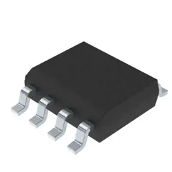
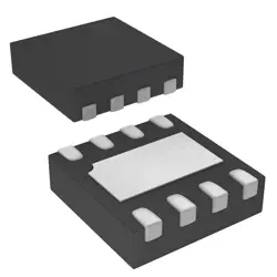
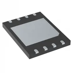
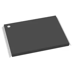
圖片僅供參考
CY2890-F02
- 製造商
- 製造商。 部分 #CY2890-F02
- 包
- 資料表
- 有現貨的9058
100%原創; 新
24小時準備發貨
365天保修
RFQ&; 獲得更多折扣
規格
| Manufacturer | JLCPCB Assembly |
| Package | LQFP-64_L7.0-W7.0-P0.40-LS9.0-BL |
概述
Description
CY2890-F02 is a highly integrated clock generator and frequency synthesizer designed for various applications in the electronics and telecommunications sectors. It offers precise timing solutions by generating multiple output frequencies from a single reference clock. The device typically features low jitter performance, making it suitable for high-speed data transfer applications.
Key features include programmable output frequencies, low power consumption, and flexibility in configuration, allowing it to cater to different system requirements. It supports various interfaces for easy integration with microcontrollers and other digital systems. The CY2890-F02 is often used in applications such as networking equipment, high-speed computing, and consumer electronics, where accurate timing is crucial for optimal performance. Overall, it provides a reliable solution for designers looking to implement robust timing circuits in their products.
Key features include programmable output frequencies, low power consumption, and flexibility in configuration, allowing it to cater to different system requirements. It supports various interfaces for easy integration with microcontrollers and other digital systems. The CY2890-F02 is often used in applications such as networking equipment, high-speed computing, and consumer electronics, where accurate timing is crucial for optimal performance. Overall, it provides a reliable solution for designers looking to implement robust timing circuits in their products.
Features
The CY2890-F02 is an advanced clock generator and synthesizer designed for high-performance applications. Key features include:
1. Frequency Range: It supports a wide frequency range, typically from 1 MHz to several hundred MHz, allowing it to generate various clock frequencies.
2. Low Jitter: The device offers low phase noise and jitter performance, making it ideal for high-speed data communication systems.
3. Multiple Output Clocks: It can provide multiple clock outputs, allowing for synchronization across different components within a system.
4. Programmability: The CY2890-F02 is programmable via I2C or SPI interfaces, enabling easy configuration and integration into custom applications.
5. Power Efficiency: Designed for low power consumption, it helps in reducing overall system energy usage.
6. Compact Package: The device is available in a compact package, facilitating easy integration into space-constrained designs.
These features make the CY2890-F02 suitable for applications in telecommunications, data centers, and embedded systems.
1. Frequency Range: It supports a wide frequency range, typically from 1 MHz to several hundred MHz, allowing it to generate various clock frequencies.
2. Low Jitter: The device offers low phase noise and jitter performance, making it ideal for high-speed data communication systems.
3. Multiple Output Clocks: It can provide multiple clock outputs, allowing for synchronization across different components within a system.
4. Programmability: The CY2890-F02 is programmable via I2C or SPI interfaces, enabling easy configuration and integration into custom applications.
5. Power Efficiency: Designed for low power consumption, it helps in reducing overall system energy usage.
6. Compact Package: The device is available in a compact package, facilitating easy integration into space-constrained designs.
These features make the CY2890-F02 suitable for applications in telecommunications, data centers, and embedded systems.
Package
The CY2890-F02 is packaged in a 16-pin TSSOP (Thin Shrink Small Outline Package). This surface-mount package type is designed for compact applications and offers a low profile for space-constrained environments.
Pinout
The CY2890-F02 is a clock generator IC from Cypress Semiconductor. It features a 20-pin package and is designed for high-performance clock generation and distribution. The pin functions include:
1. Power Supply Pins: VDD (power supply) and GND (ground).
2. Input Pins: These include reference clock inputs.
3. Output Pins: Multiple clock output pins that provide various clock frequencies.
4. Control Pins: Pins for configuration and control, including programmable output settings.
5. Feedback Pins: For frequency control and phase-lock feedback.
The device supports multiple clock outputs and configurations, making it useful in applications requiring precise clock signals. It can generate different frequencies using a low-jitter clock architecture, suitable for telecommunications and networking applications.
1. Power Supply Pins: VDD (power supply) and GND (ground).
2. Input Pins: These include reference clock inputs.
3. Output Pins: Multiple clock output pins that provide various clock frequencies.
4. Control Pins: Pins for configuration and control, including programmable output settings.
5. Feedback Pins: For frequency control and phase-lock feedback.
The device supports multiple clock outputs and configurations, making it useful in applications requiring precise clock signals. It can generate different frequencies using a low-jitter clock architecture, suitable for telecommunications and networking applications.
Manufacturer
The CY2890-F02 is manufactured by Cypress Semiconductor, a company that specializes in semiconductor products. Cypress, now a part of Infineon Technologies, is known for its extensive portfolio, which includes microcontrollers, memory products, and programmable systems on chip (SoCs). Founded in 1982, Cypress has positioned itself as a key player in the embedded solutions market, particularly for applications in automotive, industrial, consumer electronics, and IoT. The CY2890-F02 specifically is a precision clock generator, designed to provide accurate timing solutions in various electronic systems. The company emphasizes innovation and high-performance products, catering to a broad range of industries.
Application
The CY2890-F02 is primarily used in precision timing applications, such as clock generation and synchronization in telecommunications, automotive systems, and industrial automation. It serves in high-performance computing, networking equipment, and consumer electronics for accurate frequency control. Additionally, it can be utilized in test and measurement equipment to ensure reliable performance in various electronic systems.
Equivalent
The CY2890-F02 chip is a precision clock generator, often used in telecommunications and networking applications. Equivalent products include:
1. Si5351A from Silicon Labs
2. LMK04800 from Texas Instruments
3. ICS8411 from Integrated Device Technology (IDT)
4. MAX5969 from Maxim Integrated
Always check specific datasheets for compatibility in terms of frequency range, output type, and other specifications.
1. Si5351A from Silicon Labs
2. LMK04800 from Texas Instruments
3. ICS8411 from Integrated Device Technology (IDT)
4. MAX5969 from Maxim Integrated
Always check specific datasheets for compatibility in terms of frequency range, output type, and other specifications.
船舶
運輸管道我們
通過DHL、FedEx、TNT、UPS或您選擇的任何其他貨運代理提供全球運輸服務。
運費參攷(DHL/FedEx):
動態主要裝載: 運費從25美元到45美元(0.5公斤)不等,預計交貨時間為2-5個工作日。
聯邦快遞: 運費從25美元到40美元(0.5公斤)不等,預計交貨時間為3-7個工作日。
不斷電供應系統: 運費從25美元到45美元(0.5公斤)不等,預計交貨時間為3-7個工作日。
三硝基甲苯: 運費從25美元到65美元(0.5公斤)不等,預計交貨時間為3-7個工作日。
增强型短消息: 運費從30美元到50美元(0.5公斤)不等,預計交貨時間為7-15個工作日。
掛號: 運費為2-4美元(0.1公斤),預計交貨時間為5-20個工作日。
支付
Payment Methods
付款條件為100%預付。
現時,我們只接受以下付款方式:
1. 貝寶
2. 信用卡/借記卡
3. 電匯
類似的
-
![MX25R8035FM1IL0]() MX25R8035FM1IL0
MX25R8035FM1IL0
Macronix
-
![MX25V1635FZNQ03]() MX25V1635FZNQ03
MX25V1635FZNQ03
Macronix
-
![MX30LF2G28AD-TI]() MX30LF2G28AD-TI
MX30LF2G28AD-TI
Macronix
-
![MX25L8035EM2I-10G]() MX25L8035EM2I-10G
MX25L8035EM2I-10G
Macronix
-
![MX25U25643GZNI00]() MX25U25643GZNI00
MX25U25643GZNI00
Macronix
-
![MX25V1635FM2I]() MX25V1635FM2I
MX25V1635FM2I
Macronix
-
![MX25U3232FZBI02]() MX25U3232FZBI02
MX25U3232FZBI02
Macronix
-
![MX25L6433FM2I-08G]() MX25L6433FM2I-08G
MX25L6433FM2I-08G
Macronix
-
![MX25U6435FM2I-10G]() MX25U6435FM2I-10G
MX25U6435FM2I-10G
Macronix
-
![MX25L12833FZ2I-10G]() MX25L12833FZ2I-10..
MX25L12833FZ2I-10..
Macronix
-
![MX25L12835FZ2I-10G]() MX25L12835FZ2I-10..
MX25L12835FZ2I-10..
Macronix
-
![MX29LV160DTTI-70G]() MX29LV160DTTI-70G
MX29LV160DTTI-70G
Macronix