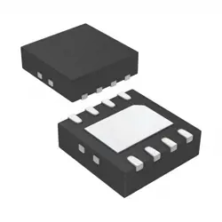
圖片僅供參考
CY14B101LA-SP45XI
IC NVSRAM 1MBIT PARALLEL 48SSOP
- 製造商
- 製造商。 部分 #CY14B101LA-SP45XI
- 包
- 資料表 CY14B101LA-SP45XI DataSheet
- 有現貨的9581
100%原創; 新
24小時準備發貨
365天保修
RFQ&; 獲得更多折扣
規格
| Part Status | Active |
| DigiKey Programmable | Not Verified |
| Memory Type | Non-Volatile |
| Memory Format | NVSRAM |
| Technology | NVSRAM (Non-Volatile SRAM) |
| Memory Size | 1Mbit |
| Memory Organization | 128K x 8 |
| Memory Interface | Parallel |
| Write Cycle Time - Word, Page | 45ns |
| Voltage - Supply | 2.7V ~ 3.6V |
| Operating Temperature | -40°C ~ 85°C (TA) |
| Mounting Type | Surface Mount |
| Package / Case | 48-BSSOP (0.295", 7.50mm Width) |
| Supplier Device Package | 48-SSOP |
| Base Product Number | CY14B101 |
| Access Time | 45 ns |
概述
Description
The CY14B101LA-SP45XI is a non-volatile memory device from Cypress Semiconductor, specifically a Serial NOR Flash memory. This device features a 1 Megabit (128 KB) storage capacity and is designed for applications requiring data retention without power. It typically utilizes the SPI (Serial Peripheral Interface) protocol, enabling fast and efficient data transfer between the memory and microcontrollers or other digital devices. The "SP45" in the part number indicates specific speed and performance characteristics, while the "XI" denotes a specific temperature range and packaging suitable for various industrial applications. Key features include low power consumption, high endurance, and reliability, making it suitable for use in embedded systems, automotive, and consumer electronics where data integrity and retention are critical. Overall, the CY14B101LA-SP45XI is an ideal choice for developers seeking a compact, efficient solution for non-volatile storage needs.
Features
The CY14B101LA-SP45XI is a 1-Mbit (128 K x 8) Serial EEPROM (Electrically Erasable Programmable Read-Only Memory) device manufactured by Cypress Semiconductor. Key features include:
1. Interface: It uses a Serial Peripheral Interface (SPI) for fast data transfers.
2. High Speed: The device supports clock rates up to 45 MHz, enabling quick access times.
3. Endurance: Offers up to 1 million write/erase cycles, ensuring durability for applications requiring frequent updates.
4. Data Retention: Retains data for over 100 years, making it suitable for long-term storage applications.
5. Low Power Consumption: Operates at low voltage (2.7V to 3.6V) and consumes minimal power in standby and active modes.
6. Package Options: Available in various packages, including SOIC and TSSOP, facilitating integration into different designs.
7. Security Features: Includes write protection and locking capabilities to secure stored data.
This combination of features makes the CY14B101LA-SP45XI ideal for applications in industrial, automotive, and consumer electronics.
1. Interface: It uses a Serial Peripheral Interface (SPI) for fast data transfers.
2. High Speed: The device supports clock rates up to 45 MHz, enabling quick access times.
3. Endurance: Offers up to 1 million write/erase cycles, ensuring durability for applications requiring frequent updates.
4. Data Retention: Retains data for over 100 years, making it suitable for long-term storage applications.
5. Low Power Consumption: Operates at low voltage (2.7V to 3.6V) and consumes minimal power in standby and active modes.
6. Package Options: Available in various packages, including SOIC and TSSOP, facilitating integration into different designs.
7. Security Features: Includes write protection and locking capabilities to secure stored data.
This combination of features makes the CY14B101LA-SP45XI ideal for applications in industrial, automotive, and consumer electronics.
Package
The CY14B101LA-SP45XI is packaged in a 10-lead, 8mm x 6mm TDFN (Thin Dual Flat No-lead) package. This compact form factor is designed for space-constrained applications while ensuring reliable performance for memory functions.
Pinout
The CY14B101LA-SP45XI is a 1 Megabit (128K x 8) Non-Volatile Static RAM (NVRAM) with a pin count of 32 in a TSOP package.
Pin Functions:
1. Address Pins (A0-A16): Used to select memory locations.
2. Data Pins (D0-D7): Bi-directional data bus for read and write operations.
3. Chip Enable (CE): Activates the device for read/write operations.
4. Write Enable (WE): Controls write operations; active low.
5. Output Enable (OE): Controls the output drivers; active low.
6. VCC: Power supply pin.
7. VSS: Ground reference.
8. WP (Write Protect): Used to enable or disable write operations.
This device combines SRAM speed with non-volatility, making it suitable for applications requiring fast access and data retention without power.
Pin Functions:
1. Address Pins (A0-A16): Used to select memory locations.
2. Data Pins (D0-D7): Bi-directional data bus for read and write operations.
3. Chip Enable (CE): Activates the device for read/write operations.
4. Write Enable (WE): Controls write operations; active low.
5. Output Enable (OE): Controls the output drivers; active low.
6. VCC: Power supply pin.
7. VSS: Ground reference.
8. WP (Write Protect): Used to enable or disable write operations.
This device combines SRAM speed with non-volatility, making it suitable for applications requiring fast access and data retention without power.
Manufacturer
The CY14B101LA-SP45XI is manufactured by Cypress Semiconductor, a company known for its development and production of advanced semiconductor solutions. Cypress, which is now part of Infineon Technologies following its acquisition in 2020, specializes in a range of products including memory, microcontrollers, and connectivity solutions for various applications. The CY14B101LA-SP45XI is a Serial NOR Flash memory device, typically used in automotive and industrial applications due to its high reliability and performance. Cypress is recognized for its innovation in the semiconductor industry, particularly in areas such as embedded memory and mixed-signal solutions.
Application
The CY14B101LA-SP45XI is a non-volatile static random-access memory (NVRAM) device primarily used in applications requiring data retention without power. Common application areas include automotive systems, industrial automation, medical devices, and consumer electronics, where it is utilized for storing configuration settings, critical data, and firmware. Its features make it suitable for environments with high reliability and endurance requirements.
Equivalent
The CY14B101LA-SP45XI chip is a 1-Mbit (128K x 8) serial NOR Flash memory. Equivalent products include:
1. Microchip SST26VF010B
2. Winbond W25Q16JV
3. Adesto AT25DF041A
4. GigaDevice GD25Q16C
Always verify compatibility based on specific application requirements such as voltage, speed, and packaging.
1. Microchip SST26VF010B
2. Winbond W25Q16JV
3. Adesto AT25DF041A
4. GigaDevice GD25Q16C
Always verify compatibility based on specific application requirements such as voltage, speed, and packaging.
船舶
運輸管道我們
通過DHL、FedEx、TNT、UPS或您選擇的任何其他貨運代理提供全球運輸服務。
運費參攷(DHL/FedEx):
動態主要裝載: 運費從25美元到45美元(0.5公斤)不等,預計交貨時間為2-5個工作日。
聯邦快遞: 運費從25美元到40美元(0.5公斤)不等,預計交貨時間為3-7個工作日。
不斷電供應系統: 運費從25美元到45美元(0.5公斤)不等,預計交貨時間為3-7個工作日。
三硝基甲苯: 運費從25美元到65美元(0.5公斤)不等,預計交貨時間為3-7個工作日。
增强型短消息: 運費從30美元到50美元(0.5公斤)不等,預計交貨時間為7-15個工作日。
掛號: 運費為2-4美元(0.1公斤),預計交貨時間為5-20個工作日。
支付
Payment Methods
付款條件為100%預付。
現時,我們只接受以下付款方式:
1. 貝寶
2. 信用卡/借記卡
3. 電匯
類似的
-
![MX25R8035FM1IL0]() MX25R8035FM1IL0
MX25R8035FM1IL0
Macronix
-
![MX25L3233FZBI-08Q]() MX25L3233FZBI-08Q
MX25L3233FZBI-08Q
Macronix
-
![MX25L3233FM1I-08Q]() MX25L3233FM1I-08Q
MX25L3233FM1I-08Q
Macronix
-
![MX25V1635FZNI]() MX25V1635FZNI
MX25V1635FZNI
Macronix
-
![MX66U1G45GXDI00]() MX66U1G45GXDI00
MX66U1G45GXDI00
Macronix
-
![MX25V5126FM1I]() MX25V5126FM1I
MX25V5126FM1I
Macronix
-
![MX25V4035FZUI]() MX25V4035FZUI
MX25V4035FZUI
Macronix
-
![MX25V16066M1I02]() MX25V16066M1I02
MX25V16066M1I02
Macronix
-
![MX25L25673GMI-08G]() MX25L25673GMI-08G
MX25L25673GMI-08G
Macronix
-
![MX25U25643GZNI00]() MX25U25643GZNI00
MX25U25643GZNI00
Macronix
-
![MX25L12833FM2I-10G]() MX25L12833FM2I-10..
MX25L12833FM2I-10..
Macronix
-
![MX25L12833FZNI-10G]() MX25L12833FZNI-10..
MX25L12833FZNI-10..
Macronix