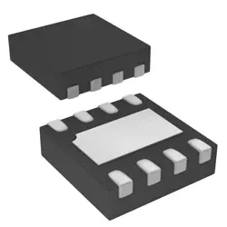
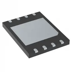
圖片僅供參考
CSD87333Q3D
MOSFET 2N-CH 30V 15A 8SON
- 製造商
- 製造商。 部分 #CSD87333Q3D
- 包 8-PowerTDFN
- 資料表 CSD87333Q3D DataSheet
- 有現貨的2668
100%原創; 新
24小時準備發貨
365天保修
RFQ&; 獲得更多折扣
規格
| Supplier | Texas Instruments |
| Package | Tape & Reel (TR),Cut Tape (CT) |
| Series | NexFET™ |
| ProductStatus | Active |
| FETType | 2 N-Channel (Dual) Asymmetrical |
| FETFeature | Logic Level Gate, 5V Drive |
| DraintoSourceVoltage(Vdss) | 30V |
| Current-ContinuousDrain(Id)@25°C | 15A |
| RdsOn(Max)@IdVgs | 14.3mOhm @ 4A, 8V |
| Vgs(th)(Max)@Id | 1.2V @ 250µA |
| GateCharge(Qg)(Max)@Vgs | 4.6nC @ 4.5V |
| InputCapacitance(Ciss)(Max)@Vds | 662pF @ 15V |
| Power-Max | 6W |
| OperatingTemperature | 125°C (TJ) |
| MountingType | Surface Mount |
| Package/Case | 8-PowerTDFN |
概述
Description
CSD87333Q3D is TI’s NexFET dual N-channel power MOSFET in a 3x3 mm QFN (Q3D) package, automotive-qualified for harsh environments. It contains two N-channel FETs rated for roughly 30 V with low on-resistance (typical around tens of milliohms per FET) and fast switching, optimized for high-efficiency switching regulators.
Key points:
- Package: QFN-3x3 with exposed pad for heat dissipation
- Rating: about 30 V, dual N-channel devices
- Resistance: typically tens of mΩ per FET
- Features: low gate charge, suitable for synchronous buck/converter use
- Applications: automotive and industrial DC-DC converters, power management, half-bridge topologies
- Use: connect as a high-side/low-side pair per datasheet; ensure proper gate drive voltage and thermal management
For exact electrical specs, recommended operating conditions, and PCB footprint, consult the TI datasheet.
Key points:
- Package: QFN-3x3 with exposed pad for heat dissipation
- Rating: about 30 V, dual N-channel devices
- Resistance: typically tens of mΩ per FET
- Features: low gate charge, suitable for synchronous buck/converter use
- Applications: automotive and industrial DC-DC converters, power management, half-bridge topologies
- Use: connect as a high-side/low-side pair per datasheet; ensure proper gate drive voltage and thermal management
For exact electrical specs, recommended operating conditions, and PCB footprint, consult the TI datasheet.
Features
Here are the typical features of TI CSD87333Q3D (Automotive-grade) at a glance:
- Automotive-grade, Q3D—AEC-Q100 compliant package
- Synchronous buck regulator with integrated high-side and low-side MOSFETs
- Wide input voltage range (suitable for 12/24V automotive rails)
- Adjustable output via external feedback (and fixed-output variants may exist)
- Soft-start and enable pin; power-good/reset signaling
- Current-mode control with PWM operation
- Protections: overcurrent/short-circuit protection, thermal shutdown, undervoltage lockout
- High efficiency благодаря synchronous topology
- Small 3×3 mm QFN package with exposed pad for thermal dissipation
Note: exact output voltage options, switching frequency, and pinout may vary by specific variant. For precise specs, consult the TI datasheet for CSD87333Q3D.
- Automotive-grade, Q3D—AEC-Q100 compliant package
- Synchronous buck regulator with integrated high-side and low-side MOSFETs
- Wide input voltage range (suitable for 12/24V automotive rails)
- Adjustable output via external feedback (and fixed-output variants may exist)
- Soft-start and enable pin; power-good/reset signaling
- Current-mode control with PWM operation
- Protections: overcurrent/short-circuit protection, thermal shutdown, undervoltage lockout
- High efficiency благодаря synchronous topology
- Small 3×3 mm QFN package with exposed pad for thermal dissipation
Note: exact output voltage options, switching frequency, and pinout may vary by specific variant. For precise specs, consult the TI datasheet for CSD87333Q3D.
Package
CSD87333Q3D is in an 8‑pin QFN package (3.0 x 3.0 mm) with an exposed pad.
Pinout
Pin count: 16 pins in a 3.0 × 3.0 mm QFN package, plus an exposed pad (center pad).
Function: Dual N-channel MOSFET pair intended for power switching (high-side and low-side) in synchronous buck converters. Each FET has its own gate; drains are commonly tied to the package center pad (and/or dedicated drain pins per package variant), with sources connected to the respective nodes. For exact pinout and wiring, see the CSD87333Q3D datasheet.
Function: Dual N-channel MOSFET pair intended for power switching (high-side and low-side) in synchronous buck converters. Each FET has its own gate; drains are commonly tied to the package center pad (and/or dedicated drain pins per package variant), with sources connected to the respective nodes. For exact pinout and wiring, see the CSD87333Q3D datasheet.
Manufacturer
- Manufacturer: Texas Instruments (TI)
- What kind of company: American multinational semiconductor company that designs and manufactures analog, embedded processing, and other integrated circuits and components.
- What kind of company: American multinational semiconductor company that designs and manufactures analog, embedded processing, and other integrated circuits and components.
Application
Applications of CSD87333Q3D:
- Synchronous buck DC-DC converter power stage for VRMs in CPUs/GPUs/FPGAs/SoCs
- Automotive 12V/24V power networks as load-switch and PWM switching devices
- Motor control for BLDC/PMSM drives
- High-efficiency switching regulators in telecom and industrial equipment
- Point-of-load power management in battery-powered devices
- Synchronous buck DC-DC converter power stage for VRMs in CPUs/GPUs/FPGAs/SoCs
- Automotive 12V/24V power networks as load-switch and PWM switching devices
- Motor control for BLDC/PMSM drives
- High-efficiency switching regulators in telecom and industrial equipment
- Point-of-load power management in battery-powered devices
船舶
運輸管道我們
通過DHL、FedEx、TNT、UPS或您選擇的任何其他貨運代理提供全球運輸服務。
運費參攷(DHL/FedEx):
動態主要裝載: 運費從25美元到45美元(0.5公斤)不等,預計交貨時間為2-5個工作日。
聯邦快遞: 運費從25美元到40美元(0.5公斤)不等,預計交貨時間為3-7個工作日。
不斷電供應系統: 運費從25美元到45美元(0.5公斤)不等,預計交貨時間為3-7個工作日。
三硝基甲苯: 運費從25美元到65美元(0.5公斤)不等,預計交貨時間為3-7個工作日。
增强型短消息: 運費從30美元到50美元(0.5公斤)不等,預計交貨時間為7-15個工作日。
掛號: 運費為2-4美元(0.1公斤),預計交貨時間為5-20個工作日。
支付
Payment Methods
付款條件為100%預付。
現時,我們只接受以下付款方式:
1. 貝寶
2. 信用卡/借記卡
3. 電匯
類似的
-
![MX25V1635FZNI]() MX25V1635FZNI
MX25V1635FZNI
Macronix
-
![MX29F400CBTI-70G]() MX29F400CBTI-70G
MX29F400CBTI-70G
Macronix
-
![MX25V16066M1I02]() MX25V16066M1I02
MX25V16066M1I02
Macronix
-
![MX25V16066M2I02]() MX25V16066M2I02
MX25V16066M2I02
Macronix
-
![MX30LF2G28AD-TI]() MX30LF2G28AD-TI
MX30LF2G28AD-TI
Macronix
-
![MX25U25643GZNI00]() MX25U25643GZNI00
MX25U25643GZNI00
Macronix
-
![MX25U3232FZBI02]() MX25U3232FZBI02
MX25U3232FZBI02
Macronix
-
![MX25U6435FM2I-10G]() MX25U6435FM2I-10G
MX25U6435FM2I-10G
Macronix
-
![MX25L12833FM2I-10G]() MX25L12833FM2I-10..
MX25L12833FM2I-10..
Macronix
-
![MX25U25645GXDI00]() MX25U25645GXDI00
MX25U25645GXDI00
Macronix
-
![MX25L12835FZ2I-10G]() MX25L12835FZ2I-10..
MX25L12835FZ2I-10..
Macronix
-
![MX25L25645GXDI-08G]() MX25L25645GXDI-08..
MX25L25645GXDI-08..
Macronix