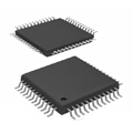
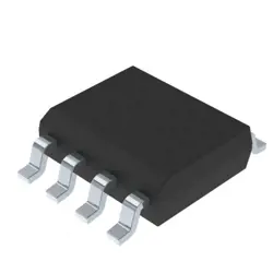
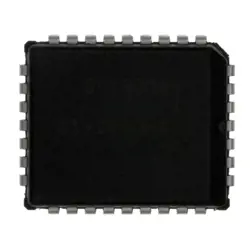
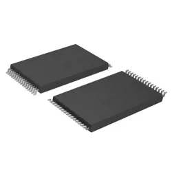
圖片僅供參考
AM29F040B-90EF
NOR Flash 4M (512Kx8) 90ns 5v Parallel NOR Flash
- 製造商
- 製造商。 部分 #AM29F040B-90EF
- 包
- 資料表 AM29F040B-90EF DataSheet
- 有現貨的22729
100%原創; 新
24小時準備發貨
365天保修
RFQ&; 獲得更多折扣
規格
| Packaging | Tray |
| Standard Pack Qty | 156 |
概述
Description
The AM29F040B-90EF is a 4 Megabit (512 K x 8) Flash memory chip produced by Advanced Micro Devices (AMD). It is designed for applications requiring non-volatile memory that can be electrically erased and reprogrammed. The device features a 90 ns access time, making it suitable for high-speed performance in embedded systems.
Key characteristics include:
- Architecture: It utilizes a 32-pin DIP or PLCC package.
- Programming: The chip supports a simple programming method using a single voltage for both programming and erasing, with a sector-based erase capability.
- Endurance: It offers a minimum of 100,000 erase/program cycles, ensuring reliability over time.
- Data Retention: The AM29F040B-90EF provides data retention of up to 20 years under typical conditions.
This Flash memory is commonly used in consumer electronics, automotive applications, and telecommunications for firmware storage and data logging. Its combination of speed, endurance, and ease of use makes it a popular choice in various electronic designs.
Features
The AM29F040B-90EF is a 4 Mbit (512 K x 8) Flash memory chip manufactured by AMD. Key features include:
1. Architecture: It utilizes a single 5V power supply and is organized as 512 Kbytes of memory.
2. Speed: The "-90" suffix indicates a maximum access time of 90 ns, allowing for fast data retrieval.
3. Data Interface: Supports a parallel data interface, enabling easy integration with various microcontrollers and processors.
4. Programming: It features a sector erase capability and supports both byte and word programming modes, allowing for flexible data manipulation.
5. Endurance: The chip has a typical endurance of up to 100,000 write/erase cycles per sector.
6. Data Retention: Offers a data retention period of up to 20 years, ensuring data stability over time.
7. Compatibility: Designed to be compatible with other industry-standard Flash memory devices, facilitating design integration.
These features make the AM29F040B-90EF suitable for applications requiring non-volatile memory storage and quick data access.
Package
The AM29F040B-90EF is packaged in a 32-pin TSOP (Thin Small Outline Package) configuration.
Pinout
The AM29F040B-90EF is a 4 megabit (512 K x 8) Flash memory chip. It has a total of 32 pins. The key functions of the pins include:
1. Address Inputs (A0-A19): Used to select the memory location.
2. Data Inputs/Outputs (DQ0-DQ7): Bidirectional data bus for reading or writing data.
3. Chip Enable (CE): Activates the chip for read/write operations.
4. Output Enable (OE): Enables the output drivers for data read.
5. Write Enable (WE): Controls write operations to the memory.
6. Reset (RESET): Resets the device to a known state.
7. VCC: Power supply pin.
8. VSS: Ground pin.
9. A-1: Used for manufacturer and device identification.
This device operates in a single +5V power supply and is typically used in applications requiring non-volatile memory, such as firmware storage.
Manufacturer
The AM29F040B-90EF is manufactured by Advanced Micro Devices, Inc. (AMD). AMD is a semiconductor company that specializes in developing computer processors and related technologies for both consumer and enterprise markets. Founded in 1969, it is known for its microprocessors, graphics processors, and other chipsets. AMD is recognized as a significant player in the computing industry, competing with other major companies like Intel and NVIDIA. The AM29F040B-90EF is a 4 Mb (512 K x 8) Flash memory device, commonly used in applications requiring non-volatile storage. AMD focuses on innovation in high-performance computing, gaming, and graphics solutions.
Application
The AM29F040B-90EF is a 4-Mbit (512 K x 8) Flash memory chip primarily used in embedded systems for applications such as BIOS storage, firmware updates, and boot code in consumer electronics, automotive systems, industrial automation, and networking devices. Its non-volatile nature makes it suitable for applications requiring data retention without power.
Equivalent
The AM29F040B-90EF is a 4Mb (512K x 8) Flash memory chip. Equivalent products include:
1. Intel 28F040
2. Microchip 25F040
3. STMicroelectronics M29F040
4. Winbond W29F040
These chips share similar specifications, including density and organization, making them suitable replacements depending on the design requirements. Always verify compatibility in specific applications.
1. Intel 28F040
2. Microchip 25F040
3. STMicroelectronics M29F040
4. Winbond W29F040
These chips share similar specifications, including density and organization, making them suitable replacements depending on the design requirements. Always verify compatibility in specific applications.
船舶
運輸管道我們
通過DHL、FedEx、TNT、UPS或您選擇的任何其他貨運代理提供全球運輸服務。
運費參攷(DHL/FedEx):
動態主要裝載: 運費從25美元到45美元(0.5公斤)不等,預計交貨時間為2-5個工作日。
聯邦快遞: 運費從25美元到40美元(0.5公斤)不等,預計交貨時間為3-7個工作日。
不斷電供應系統: 運費從25美元到45美元(0.5公斤)不等,預計交貨時間為3-7個工作日。
三硝基甲苯: 運費從25美元到65美元(0.5公斤)不等,預計交貨時間為3-7個工作日。
增强型短消息: 運費從30美元到50美元(0.5公斤)不等,預計交貨時間為7-15個工作日。
掛號: 運費為2-4美元(0.1公斤),預計交貨時間為5-20個工作日。
支付
Payment Methods
付款條件為100%預付。
現時,我們只接受以下付款方式:
1. 貝寶
2. 信用卡/借記卡
3. 電匯
類似的
-
![MX25R8035FM1IL0]() MX25R8035FM1IL0
Macronix
-
![MX25L3233FZBI-08Q]() MX25L3233FZBI-08Q
Macronix
-
![MX25V5126FM1I]() MX25V5126FM1I
Macronix
-
![MX25V4035FZUI]() MX25V4035FZUI
Macronix
-
![MX29GL512FHXFI-11G]() MX29GL512FHXFI-11..
Macronix
-
![MX25U51279GXDR00]() MX25U51279GXDR00
Macronix
-
![MX25L2006EM1I-12G]() MX25L2006EM1I-12G
Macronix
-
![MX25R1635FZUIH0]() MX25R1635FZUIH0
Macronix
-
![MX25V1635FM2I]() MX25V1635FM2I
Macronix
-
![MX25L6433FM2I-08G]() MX25L6433FM2I-08G
Macronix
-
![MX29F040CQI-70G]() MX29F040CQI-70G
Macronix
-
![MX29F040CTI-70G]() MX29F040CTI-70G
Macronix