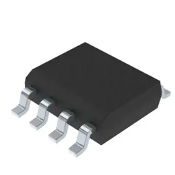
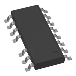
圖片僅供參考
ADC-20-12+
RF DIR CPLR 100MHZ-1.2GHZ 6SMD
- 製造商
- 製造商。 部分 #ADC-20-12+
- 包
- 資料表 ADC-20-12+ DataSheet
- 有現貨的21234
100%原創; 新
24小時準備發貨
365天保修
RFQ&; 獲得更多折扣
規格
| Part Status | Active |
| Coupler Type | Standard |
| Frequency | 100MHz ~ 1.2GHz |
| Coupling Factor | 20 ± 0.75dB |
| Applications | General Purpose |
| Power - Max | 1W |
| Return Loss | 30.72dB |
| Package / Case | 6-SMD, Flat Leads |
概述
Description
ADC-20-12+ refers to a specific type of Analog-to-Digital Converter (ADC) module or chip, typically noted for its performance features such as resolution, sampling rate, and power consumption. These specifications make it suitable for various applications in fields like telecommunications, instrumentation, and industrial control systems.
An introduction to ADC-20-12+ would cover its key characteristics, including:
- Resolution: Often 12 bits or higher, determining how finely the analog signal can be represented in digital form.
- Sampling Rate: The frequency at which the ADC samples the analog input, impacting the fidelity of the digital representation.
- Input Voltage Range: Defines the acceptable range of input voltages that can be converted.
- Interface: The type of communication protocol it uses (e.g., SPI, I2C) for integration with microcontrollers or processors.
Additionally, the ADC-20-12+ may feature noise reduction capabilities and low power operation, making it ideal for battery-powered devices. Understanding its specifications and applications is crucial for engineers looking to implement efficient data conversion solutions.
An introduction to ADC-20-12+ would cover its key characteristics, including:
- Resolution: Often 12 bits or higher, determining how finely the analog signal can be represented in digital form.
- Sampling Rate: The frequency at which the ADC samples the analog input, impacting the fidelity of the digital representation.
- Input Voltage Range: Defines the acceptable range of input voltages that can be converted.
- Interface: The type of communication protocol it uses (e.g., SPI, I2C) for integration with microcontrollers or processors.
Additionally, the ADC-20-12+ may feature noise reduction capabilities and low power operation, making it ideal for battery-powered devices. Understanding its specifications and applications is crucial for engineers looking to implement efficient data conversion solutions.
Features
The ADC-20-12+ is a high-performance analog-to-digital converter (ADC) designed for precise data acquisition in various applications. Key features include:
1. 20-Bit Resolution: Offers high precision for accurate signal representation.
2. 12 MSPS Sampling Rate: Capable of sampling at 12 million samples per second, making it suitable for high-speed applications.
3. Single-Ended and Differential Inputs: Supports both input types for flexibility in signal measurement.
4. Low Noise: Enhanced signal integrity with minimal noise interference, ideal for sensitive applications.
5. Wide Input Voltage Range: Accommodates different signal levels, increasing versatility across various systems.
6. Integrated Reference Voltage: Provides a stable reference for improved accuracy.
7. Low Power Consumption: Designed for energy efficiency, making it suitable for battery-operated devices.
8. Digital Output Interface: Typically features options like SPI or I2C for easy integration with microcontrollers or processors.
These features make the ADC-20-12+ suitable for applications in medical devices, industrial automation, and data acquisition systems.
1. 20-Bit Resolution: Offers high precision for accurate signal representation.
2. 12 MSPS Sampling Rate: Capable of sampling at 12 million samples per second, making it suitable for high-speed applications.
3. Single-Ended and Differential Inputs: Supports both input types for flexibility in signal measurement.
4. Low Noise: Enhanced signal integrity with minimal noise interference, ideal for sensitive applications.
5. Wide Input Voltage Range: Accommodates different signal levels, increasing versatility across various systems.
6. Integrated Reference Voltage: Provides a stable reference for improved accuracy.
7. Low Power Consumption: Designed for energy efficiency, making it suitable for battery-operated devices.
8. Digital Output Interface: Typically features options like SPI or I2C for easy integration with microcontrollers or processors.
These features make the ADC-20-12+ suitable for applications in medical devices, industrial automation, and data acquisition systems.
Package
The ADC-20-12+ is a DC-DC power converter from Analog Devices, typically housed in a low-profile, compact surface-mount package. Its design facilitates efficient thermal management and circuit integration.
Pinout
The ADC-20-12+ is a DC-DC converter designed by Analog Devices, featuring a pin count of 8. The pin functions are as follows:
1. Vin (Pin 1): Input voltage.
2. Vout (Pin 2): Output voltage.
3. GND (Pin 3): Ground connection.
4. Enable (EN) (Pin 4): Enables or disables the converter.
5. Comp (Pin 5): Compensation node for stability.
6. FB (Pin 6): Feedback pin for voltage regulation.
7. SW (Pin 7): Switch node for power conversion.
8. NC (Pin 8): No connection.
The ADC-20-12+ typically converts a 20V input to a 12V output, delivering a regulated output for various applications.
1. Vin (Pin 1): Input voltage.
2. Vout (Pin 2): Output voltage.
3. GND (Pin 3): Ground connection.
4. Enable (EN) (Pin 4): Enables or disables the converter.
5. Comp (Pin 5): Compensation node for stability.
6. FB (Pin 6): Feedback pin for voltage regulation.
7. SW (Pin 7): Switch node for power conversion.
8. NC (Pin 8): No connection.
The ADC-20-12+ typically converts a 20V input to a 12V output, delivering a regulated output for various applications.
Manufacturer
The ADC-20-12+ is manufactured by Analog Devices, Inc. (ADI). Analog Devices is a global leader in the design and manufacturing of high-performance analog, mixed-signal, and digital signal processing (DSP) integrated circuits. Founded in 1965 and headquartered in Norwood, Massachusetts, ADI serves various industries, including automotive, communications, consumer electronics, industrial automation, and healthcare. The company is known for its innovative solutions that enable accurate and reliable data conversion, signal processing, and sensor interfacing, making it crucial in applications that require precision and performance.
Application
The ADC-20-12+ is a high-performance RF amplifier commonly used in applications such as communication systems, radar, and signal processing. It is suitable for use in test equipment, satellite communications, and instrumentation due to its wide bandwidth, high gain, and low noise figure. Additional applications include industrial monitoring, medical imaging systems, and research in wireless technologies.
Equivalent
The ADC-20-12+ chip, a high-performance RF amplifier, has equivalent products such as the Mini-Circuits GVA-84++ and the RFMD RF2503. Other alternatives include components from Analog Devices like the AD8011 and similar amplifiers from other manufacturers that meet comparable specifications in gain, bandwidth, and frequency range. Always verify compatibility based on your specific application requirements.
船舶
運輸管道我們
通過DHL、FedEx、TNT、UPS或您選擇的任何其他貨運代理提供全球運輸服務。
運費參攷(DHL/FedEx):
動態主要裝載: 運費從25美元到45美元(0.5公斤)不等,預計交貨時間為2-5個工作日。
聯邦快遞: 運費從25美元到40美元(0.5公斤)不等,預計交貨時間為3-7個工作日。
不斷電供應系統: 運費從25美元到45美元(0.5公斤)不等,預計交貨時間為3-7個工作日。
三硝基甲苯: 運費從25美元到65美元(0.5公斤)不等,預計交貨時間為3-7個工作日。
增强型短消息: 運費從30美元到50美元(0.5公斤)不等,預計交貨時間為7-15個工作日。
掛號: 運費為2-4美元(0.1公斤),預計交貨時間為5-20個工作日。
支付
Payment Methods
付款條件為100%預付。
現時,我們只接受以下付款方式:
1. 貝寶
2. 信用卡/借記卡
3. 電匯
類似的
-
![MX29F400CBTI-70G]() MX29F400CBTI-70G
MX29F400CBTI-70G
Macronix
-
![MX25L8035EM2I-10G]() MX25L8035EM2I-10G
MX25L8035EM2I-10G
Macronix
-
![MX25R6435FBDIL0]() MX25R6435FBDIL0
MX25R6435FBDIL0
Macronix
-
![MX25L25673GMI-10G]() MX25L25673GMI-10G
MX25L25673GMI-10G
Macronix
-
![MX25U25643GZNI00]() MX25U25643GZNI00
MX25U25643GZNI00
Macronix
-
![MX25L2006EM1I-12G]() MX25L2006EM1I-12G
MX25L2006EM1I-12G
Macronix
-
![MX25V1635FM2I]() MX25V1635FM2I
MX25V1635FM2I
Macronix
-
![MX25U25645GXDI00]() MX25U25645GXDI00
MX25U25645GXDI00
Macronix
-
![MX25L25645GXDI-08G]() MX25L25645GXDI-08..
MX25L25645GXDI-08..
Macronix
-
![MX29LV640ETTI-70G]() MX29LV640ETTI-70G
MX29LV640ETTI-70G
Macronix
-
![MX25L25735FMI-10G]() MX25L25735FMI-10G
MX25L25735FMI-10G
Macronix
-
![MX25L1006EMI-10G]() MX25L1006EMI-10G
MX25L1006EMI-10G
Macronix