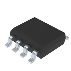
圖片僅供參考
74LVC1G125SE-7
IC BUFF NON-INVERT 5.5V SOT-353
- 製造商
- 製造商。 部分 #74LVC1G125SE-7
- 包
- 資料表 74LVC1G125SE-7 DataSheet
- 有現貨的2430
100%原創; 新
24小時準備發貨
365天保修
RFQ&; 獲得更多折扣
規格
| Series | 74LVC |
| Part Status | Active |
| Base Product Number | 74LVC1G125 |
| Logic Type | Buffer, Non-Inverting |
| Number of Elements | 1 |
| Number of Bits per Element | 1 |
| Output Type | 3-State |
| Current - Output High, Low | 32mA, 32mA |
| Voltage - Supply | 1.65V ~ 5.5V |
| Operating Temperature | -40°C ~ 125°C (TA) |
| Mounting Type | Surface Mount |
| Package | 5-TSSOP, SC-70-5, SOT-353 |
| Supplier Device Package | SOT-353 |
| Packaging | Cut Tape (CT), Tape & Reel (TR) |
概述
Description
74LVC1G125SE-7 is a single-channel, non-inverting buffer with tri-state output in the 74LVC1G125 family. It buffers input A to output Y when the output enable (/OE) is asserted (low); when /OE is deasserted (high), the output is high-impedance. It operates from a 1.65–3.6 V supply and provides rail-to-rail I/O with low static power.
Key points:
- 1-channel buffer with 3-state output
- Active-low enable (/OE)
- Vcc range: 1.65–3.6 V
- Small SE package (SC-70/SOT-23 style) suitable for compact boards
- Used for bus sharing, level-bridging within the supply range, and buffering signals from a MCU/FPGA
Pinout (typical): A (input), Y (output), /OE (enable), Vcc, GND. For exact electrical specs (V_IH/IL, V_OH/OL, I_O, t_pd) and precise package details, consult the TI datasheet for 74LVC1G125SE-7.
Key points:
- 1-channel buffer with 3-state output
- Active-low enable (/OE)
- Vcc range: 1.65–3.6 V
- Small SE package (SC-70/SOT-23 style) suitable for compact boards
- Used for bus sharing, level-bridging within the supply range, and buffering signals from a MCU/FPGA
Pinout (typical): A (input), Y (output), /OE (enable), Vcc, GND. For exact electrical specs (V_IH/IL, V_OH/OL, I_O, t_pd) and precise package details, consult the TI datasheet for 74LVC1G125SE-7.
Features
Here are the key features of 74LVC1G125SE-7:
- Single-bit buffer/line driver with 3-state output
- Output enable (OE) input to control high-impedance state
- Supply voltage: Vcc = 1.65 V to 3.6 V (LVC family)
- CMOS/TTL-compatible input thresholds
- Ioff support (partial-power-down) for safe operation with powered-down devices
- Low static and dynamic power; high-speed CMOS performance
- Small SE-7 package (SC-70 family) with RoHS/compliant packaging
(Notes: OE enables the output when asserted; when not enabled, the output is high-impedance.)
- Single-bit buffer/line driver with 3-state output
- Output enable (OE) input to control high-impedance state
- Supply voltage: Vcc = 1.65 V to 3.6 V (LVC family)
- CMOS/TTL-compatible input thresholds
- Ioff support (partial-power-down) for safe operation with powered-down devices
- Low static and dynamic power; high-speed CMOS performance
- Small SE-7 package (SC-70 family) with RoHS/compliant packaging
(Notes: OE enables the output when asserted; when not enabled, the output is high-impedance.)
Package
SC-70-5 (5-pin) package, a tiny SC-70 style SMD package.
Pinout
- Pin count: 5 pins
- Function: Single non‑inverting buffer with a 3‑state (tri‑state) output. Pins: A (input), Y (output), G (output enable), Vcc, GND.
- Function: Single non‑inverting buffer with a 3‑state (tri‑state) output. Pins: A (input), Y (output), G (output enable), Vcc, GND.
Manufacturer
- Manufacturer: Nexperia
- What kind of company: A global semiconductor company (Dutch-based) that designs and manufactures discrete components and logic/mosfet devices.
- What kind of company: A global semiconductor company (Dutch-based) that designs and manufactures discrete components and logic/mosfet devices.
Application
74LVC1G125SE-7 is a single-bit, non-inverting buffer with a 3-state output (OE).
Applications:
- Buffers for high-speed digital signals between ICs (MCUs, FPGAs, ASICs)
- Shared-bus interfaces with tri-state control to enable/disable drivers
- Level shifting / voltage-domain isolation between different logic levels
- Drive and condition signals for memory interfaces (SRAM, registers) and peripherals
- General I/O expansion and signal integrity improvement in digital designs
Applications:
- Buffers for high-speed digital signals between ICs (MCUs, FPGAs, ASICs)
- Shared-bus interfaces with tri-state control to enable/disable drivers
- Level shifting / voltage-domain isolation between different logic levels
- Drive and condition signals for memory interfaces (SRAM, registers) and peripherals
- General I/O expansion and signal integrity improvement in digital designs
Equivalent
Likely equivalents (same function: 1-bit, non-inverting buffer with 3‑state output in the LVC family):
- TI SN74LVC1G125 (same device family)
- NXP/Nexperia 74LVC1G125
- Diodes Incorporated ALVC1G125
- Onsemi NC7WZ125 or NC7SZ125 (functional cross‑reference 3‑state buffer)
Note: packaging and temp grades may vary; check voltage range and acceptable packages for your design.
- TI SN74LVC1G125 (same device family)
- NXP/Nexperia 74LVC1G125
- Diodes Incorporated ALVC1G125
- Onsemi NC7WZ125 or NC7SZ125 (functional cross‑reference 3‑state buffer)
Note: packaging and temp grades may vary; check voltage range and acceptable packages for your design.
船舶
運輸管道我們
通過DHL、FedEx、TNT、UPS或您選擇的任何其他貨運代理提供全球運輸服務。
運費參攷(DHL/FedEx):
動態主要裝載: 運費從25美元到45美元(0.5公斤)不等,預計交貨時間為2-5個工作日。
聯邦快遞: 運費從25美元到40美元(0.5公斤)不等,預計交貨時間為3-7個工作日。
不斷電供應系統: 運費從25美元到45美元(0.5公斤)不等,預計交貨時間為3-7個工作日。
三硝基甲苯: 運費從25美元到65美元(0.5公斤)不等,預計交貨時間為3-7個工作日。
增强型短消息: 運費從30美元到50美元(0.5公斤)不等,預計交貨時間為7-15個工作日。
掛號: 運費為2-4美元(0.1公斤),預計交貨時間為5-20個工作日。
支付
Payment Methods
付款條件為100%預付。
現時,我們只接受以下付款方式:
1. 貝寶
2. 信用卡/借記卡
3. 電匯
類似的
-
![MX25R8035FM1IL0]() MX25R8035FM1IL0
MX25R8035FM1IL0
Macronix
-
![MX25L3233FZBI-08Q]() MX25L3233FZBI-08Q
MX25L3233FZBI-08Q
Macronix
-
![MX29F400CBTI-70G]() MX29F400CBTI-70G
MX29F400CBTI-70G
Macronix
-
![MX66U1G45GXDI00]() MX66U1G45GXDI00
MX66U1G45GXDI00
Macronix
-
![MX25V4035FZUI]() MX25V4035FZUI
MX25V4035FZUI
Macronix
-
![MX25V16066M1I02]() MX25V16066M1I02
MX25V16066M1I02
Macronix
-
![MX25R3235FZNIL0]() MX25R3235FZNIL0
MX25R3235FZNIL0
Macronix
-
![MX30LF2G28AD-TI]() MX30LF2G28AD-TI
MX30LF2G28AD-TI
Macronix
-
![MX25L8035EM2I-10G]() MX25L8035EM2I-10G
MX25L8035EM2I-10G
Macronix
-
![MX25L25673GMI-10G]() MX25L25673GMI-10G
MX25L25673GMI-10G
Macronix
-
![MX25V1635FM2I]() MX25V1635FM2I
MX25V1635FM2I
Macronix
-
![MX25L12833FM2I-10G]() MX25L12833FM2I-10..
MX25L12833FM2I-10..
Macronix