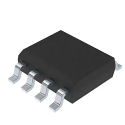
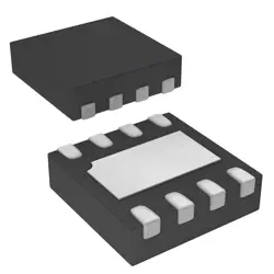
圖片僅供參考
74HCT2G125DP
Nexperia
- 製造商
- 製造商。 部分 #74HCT2G125DP
- 包
- 資料表
- 有現貨的13989
100%原創; 新
24小時準備發貨
365天保修
RFQ&; 獲得更多折扣
規格
概述
Description
The 74HCT2G125DP is a dual buffer/driver with a 3-state output, part of the 74HCT logic family, which operates with a supply voltage of 2V to 6V. It is designed for high-speed and low-power applications, making it suitable for interfacing with high-speed digital circuits. The device features two identical circuits, each with a single input and output that can be enabled or disabled, allowing for flexible configurations in digital designs.
The 74HCT2G125DP accepts standard TTL input levels and delivers output levels compatible with CMOS logic. Its 3-state output can be utilized in bus systems, enabling multiple devices to share a common data line without interference. The device is housed in a compact SOT-23 package, enhancing space efficiency in printed circuit boards (PCBs).
Overall, the 74HCT2G125DP is ideal for applications in signal buffering, data transmission, and logic level shifting within electronic systems.
The 74HCT2G125DP accepts standard TTL input levels and delivers output levels compatible with CMOS logic. Its 3-state output can be utilized in bus systems, enabling multiple devices to share a common data line without interference. The device is housed in a compact SOT-23 package, enhancing space efficiency in printed circuit boards (PCBs).
Overall, the 74HCT2G125DP is ideal for applications in signal buffering, data transmission, and logic level shifting within electronic systems.
Features
The 74HCT2G125DP is a dual buffer/driver with 3-state outputs, designed for high-speed performance in digital applications. Key features include:
1. Voltage Range: Operates within a supply voltage of 2V to 6V, compatible with both TTL and CMOS logic levels.
2. Input and Output Compatibility: Accepts standard TTL inputs while offering CMOS output characteristics, enhancing integration with various logic families.
3. High Speed: Offers fast propagation delay, typically around 5 ns at 5V, suitable for high-frequency applications.
4. Low Power Consumption: Consumes minimal power in static and dynamic states, making it ideal for battery-operated devices.
5. 3-State Outputs: Each output can be individually enabled or disabled, allowing for easy bus interfacing and preventing conflicts.
6. Temperature Range: Operates reliably over a wide temperature range, usually from -40°C to +125°C.
7. Package Options: Available in various package types, including smaller footprints, for space-constrained applications.
These features make the 74HCT2G125DP suitable for various applications in consumer electronics, automotive, and industrial systems.
1. Voltage Range: Operates within a supply voltage of 2V to 6V, compatible with both TTL and CMOS logic levels.
2. Input and Output Compatibility: Accepts standard TTL inputs while offering CMOS output characteristics, enhancing integration with various logic families.
3. High Speed: Offers fast propagation delay, typically around 5 ns at 5V, suitable for high-frequency applications.
4. Low Power Consumption: Consumes minimal power in static and dynamic states, making it ideal for battery-operated devices.
5. 3-State Outputs: Each output can be individually enabled or disabled, allowing for easy bus interfacing and preventing conflicts.
6. Temperature Range: Operates reliably over a wide temperature range, usually from -40°C to +125°C.
7. Package Options: Available in various package types, including smaller footprints, for space-constrained applications.
These features make the 74HCT2G125DP suitable for various applications in consumer electronics, automotive, and industrial systems.
Package
The 74HCT2G125DP is available in a SOT-23-5 package type. This is a small, surface-mount package suitable for space-constrained applications.
Pinout
The 74HCT2G125DP is a dual buffer/driver with a 5-pin configuration for each buffer, totaling 10 pins. It features two independent non-inverting buffers. The key pin functions are as follows:
1. A1, A2: Input pins for the two buffers.
2. Y1, Y2: Output pins corresponding to the inputs A1 and A2.
3. OE (Output Enable): Active low control pin that enables the outputs when low and disables them when high.
The device operates in the High-Speed CMOS (HCT) family, compatible with TTL levels, making it suitable for various digital applications. It can drive capacitive loads and is designed for low-power consumption.
1. A1, A2: Input pins for the two buffers.
2. Y1, Y2: Output pins corresponding to the inputs A1 and A2.
3. OE (Output Enable): Active low control pin that enables the outputs when low and disables them when high.
The device operates in the High-Speed CMOS (HCT) family, compatible with TTL levels, making it suitable for various digital applications. It can drive capacitive loads and is designed for low-power consumption.
Manufacturer
The manufacturer of the 74HCT2G125DP is Texas Instruments (TI). Texas Instruments is a global semiconductor design and manufacturing company headquartered in Dallas, Texas. It specializes in a broad range of technologies, including analog, embedded processors, and digital signal processing. TI is known for producing high-performance chips used in various applications, including automotive, industrial, communication, and consumer electronics. The company focuses on innovation and has a substantial portfolio of products that cater to diverse markets. Texas Instruments has a long-standing reputation in the semiconductor industry and is recognized for its reliability and quality.
Application
The 74HCT2G125DP is a dual buffer/driver with 3-state outputs, commonly used in digital circuits for signal buffering, level shifting, and interfacing between different voltage levels. Its application areas include data communication systems, memory interfacing, automotive electronics, consumer electronics, and any design requiring controlled signal routing and buffering in microcontroller or FPGA-based projects. The tri-state feature allows for multiple outputs to connect to a shared bus, enhancing versatility in circuit design.
Equivalent
The 74HCT2G125DP is a dual buffer/driver with 3-state outputs. Equivalent products include 74HC2G125, 74HCT125, and 74HC125, which offer similar functionality but may differ in voltage levels or package types. Always verify specifications for compatibility in your specific application.
船舶
運輸管道我們
通過DHL、FedEx、TNT、UPS或您選擇的任何其他貨運代理提供全球運輸服務。
運費參攷(DHL/FedEx):
動態主要裝載: 運費從25美元到45美元(0.5公斤)不等,預計交貨時間為2-5個工作日。
聯邦快遞: 運費從25美元到40美元(0.5公斤)不等,預計交貨時間為3-7個工作日。
不斷電供應系統: 運費從25美元到45美元(0.5公斤)不等,預計交貨時間為3-7個工作日。
三硝基甲苯: 運費從25美元到65美元(0.5公斤)不等,預計交貨時間為3-7個工作日。
增强型短消息: 運費從30美元到50美元(0.5公斤)不等,預計交貨時間為7-15個工作日。
掛號: 運費為2-4美元(0.1公斤),預計交貨時間為5-20個工作日。
支付
Payment Methods
付款條件為100%預付。
現時,我們只接受以下付款方式:
1. 貝寶
2. 信用卡/借記卡
3. 電匯
類似的
-
![MX66U1G45GXDI00]() MX66U1G45GXDI00
MX66U1G45GXDI00
Macronix
-
![MX25V5126FM1I]() MX25V5126FM1I
MX25V5126FM1I
Macronix
-
![MX25V4035FZUI]() MX25V4035FZUI
MX25V4035FZUI
Macronix
-
![MX25V16066M1I02]() MX25V16066M1I02
MX25V16066M1I02
Macronix
-
![MX25R3235FZNIL0]() MX25R3235FZNIL0
MX25R3235FZNIL0
Macronix
-
![MX25L8035EM2I-10G]() MX25L8035EM2I-10G
MX25L8035EM2I-10G
Macronix
-
![MX25L25673GMI-08G]() MX25L25673GMI-08G
MX25L25673GMI-08G
Macronix
-
![MX25U25643GZNI00]() MX25U25643GZNI00
MX25U25643GZNI00
Macronix
-
![MX25V1635FM2I]() MX25V1635FM2I
MX25V1635FM2I
Macronix
-
![MX25U3232FZBI02]() MX25U3232FZBI02
MX25U3232FZBI02
Macronix
-
![MX25U6435FM2I-10G]() MX25U6435FM2I-10G
MX25U6435FM2I-10G
Macronix
-
![MX25L12833FM2I-10G]() MX25L12833FM2I-10..
MX25L12833FM2I-10..
Macronix